 ChipApex | Global Electronic Components Supplier

SEARCH
Search Product
Search Post
— IC芯片 | 连接器 | 传感器 | 被动器件 —
Search productSearch post
— IC芯片 | 连接器 | 传感器 | 被动器件 —
Consult the customer manager about the wholesale price.
consultation hotline:86-132-6715-2157
email:[email protected]
Contact the product manager for consultation. One-stop consultation is available.
Do you want a lower wholesale price? Please send us your inquiry and we will reply immediately.
SN74ACT7806-40DL is listed in the FIFOs Memory range at ChipApex. The manufacturer field lists Texas Instruments. Its product description is IC FIFO ASYNC 256X18 56SSOP. Review the specifications below when checking this part for your BOM.
The SN74ACT7806-40DL is a 256-word by 18-bit asynchronous FIFO memory manufactured using low-power advanced CMOS technology. It features independent load and unload clock inputs, allowing data rates up to 50 MHz with access times of 24 ns under a 50-pF load. The device includes full, empty, half-full, and programmable almost-full/almost-empty status flags. It operates within a supply voltage range of 4.5 V to 5.5 V and supports an operating temperature range from 0°C to 70°C.
Verify the specific suffix '40' corresponds to the required 24 ns maximum access time and 25 MHz maximum clock frequency specifications. Confirm that the SSOP-56 package meets the thermal and physical constraints of the target application. Ensure the operating environment remains within the specified 0°C to 70°C temperature range for reliable performance.
Select this component when asynchronous FIFO functionality with an 18-bit data width is required. Compare against the SN74ACT7804 and SN74ACT7814 for pin-compatible alternatives if different timing or depth characteristics are needed. Evaluate the power dissipation capacitance and supply current requirements against system power budgets.
This device belongs to Texas Instruments' Widebus family of logic products. It utilizes low-power advanced CMOS technology to achieve high speed while maintaining low static power consumption. The part is designed for parallel data transfer applications requiring fast access times and robust status flagging capabilities.
Pin-to-pin compatible substitutes include the SN74ACT7804 and SN74ACT7814. Verify that the alternative part number meets the specific timing requirements and operational voltage ranges of the design.
The offset values are programmed after reset and before the first word is written. By holding the Program Enable (PEN) input low during the first one or two rising edges of the Load Clock (LDCK), the binary value on data inputs D0–D6 is latched as the offset values.
When the OE input is high, the data outputs (Q0–Q17) enter a high-impedance state, effectively disconnecting them from the bus regardless of the internal memory state.
Explore related parts through Logic, Integrated Circuits (ICs), all product categories, ChipApex homepage.
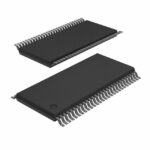 SN74ACT7806-40DL

The activity of extra discounts on wholesale prices is in full swing…
Please fill in your contact information and we will send you the latest wholesale price list.





