 ChipApex | Global Electronic Components Supplier

SEARCH
Search Product
Search Post
— IC芯片 | 连接器 | 传感器 | 被动器件 —
Search productSearch post
— IC芯片 | 连接器 | 传感器 | 被动器件 —
Consult the customer manager about the wholesale price.
consultation hotline:86-132-6715-2157
email:[email protected]
Contact the product manager for consultation. One-stop consultation is available.
Do you want a lower wholesale price? Please send us your inquiry and we will reply immediately.
SN74ACT7807-20PAG is listed in the FIFOs Memory range at ChipApex. The manufacturer field lists Texas Instruments. Its product description is IC FIFO SYNC 2KX9 13NS 64TQFP. Review the specifications below when checking this part for your BOM.
The SN74ACT7807-20PAG is a 2048-word by 9-bit synchronous FIFO memory manufactured by Texas Instruments. It operates within a supply voltage range of 4.5 V to 5.5 V and supports data rates up to 50 MHz with a maximum access time of 13 ns. The device utilizes low-power advanced CMOS technology and features three-state outputs. It includes programmable almost-full/almost-empty flags, input-ready, output-ready, and half-full status indicators. The component is housed in a 64-pin Thin Quad Flat (PAG) package and is characterized for operation from 0°C to 70°C.
Verify the specific -20 speed grade designation matches the required 50 MHz operational frequency and 13 ns access time limits. Confirm the PAG package variant aligns with the intended 64-pin footprint requirements. Ensure the operating temperature range of 0°C to 70°C satisfies the environmental conditions of the target application design.
Select this component when a 2048 x 9 bit capacity is required with synchronous control logic. Consider the -20 speed grade if system timing demands a maximum clock frequency of 50 MHz. Evaluate the availability of the 64-pin PAG package against board space constraints compared to alternative pinouts like PLCC or LQFP.
This part belongs to the SN74ACT7807 family of clocked first-in, first-out memories. The family offers various speed grades (-15, -20, -25, -40) and package options including 44-pin PLCC and 64-pin QFP. The -20PAG suffix specifically denotes the 50 MHz performance level and the 64-pin plastic thin quad flat package configuration.
Compatible substitutes include other SN74ACT7807 speed grades such as the -15, -25, or -40 variants, provided timing margins accommodate the differences. Alternative packages like the FN or PM versions offer identical electrical functionality but require different physical footprints on the printed circuit board.
Offsets are programmed after reset and before the first write by holding the Program Enable (PEN) low while providing binary values on the data inputs during a write clock transition.
The output-ready flag goes low during reset and returns high on the third rising edge of the read clock after the first valid word is loaded into empty memory.
Explore related parts through Logic, Integrated Circuits (ICs), all product categories, ChipApex homepage.
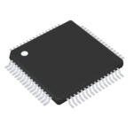 SN74ACT7807-20PAG

The activity of extra discounts on wholesale prices is in full swing…
Please fill in your contact information and we will send you the latest wholesale price list.





