 ChipApex | Global Electronic Components Supplier

SEARCH
Search Product
Search Post
— IC芯片 | 连接器 | 传感器 | 被动器件 —
Search productSearch post
— IC芯片 | 连接器 | 传感器 | 被动器件 —
Consult the customer manager about the wholesale price.
consultation hotline:86-132-6715-2157
email:[email protected]
Contact the product manager for consultation. One-stop consultation is available.
Do you want a lower wholesale price? Please send us your inquiry and we will reply immediately.
SN74AHC238BQBR is listed in the Signal Switches, Multiplexers, Decoders range at ChipApex. The manufacturer field lists Texas Instruments. Its product description is 3-LINE TO 8-LINE INVERTING AND N. Review the specifications below when checking this part for your BOM.
The SN74AHC238BQBR is a high-speed silicon gate CMOS decoder manufactured by Texas Instruments. It implements a single 3-to-8 line noninverting decoding function within a 16-pin WQFN package. The device operates across a supply voltage range of 2V to 5.5V and supports an operating temperature from -40°C to +125°C. Propagation delay reaches a maximum of 10.5ns at 5V with a 50pF load. It features balanced push-pull outputs, standard CMOS inputs, and three strobe inputs for output enable control.
Verify the specific BQB suffix indicates the WQFN package configuration. Confirm the active production status matches current design requirements. Ensure input signals transition quickly to prevent oscillations. Terminate unused inputs to VCC or GND to maintain valid logic states during operation.
Select this component when a high-speed 3-to-8 decoder is required for memory addressing or data routing. The wide supply voltage range accommodates various system power rails. The low propagation delay supports high-frequency digital interfaces. Verify that the WQFN package fits the available PCB footprint constraints.
This part belongs to the SN74AHC238 family of decoders. It serves as a core logic element for managing multiple peripheral devices on a shared bus. The device replaces older logic families by offering faster switching speeds and lower power consumption while maintaining compatible pinouts for many legacy designs.
SN74AHC238PW (TSSOP package variant)
When any of the three strobe inputs (G2, G1, or G0) are active, all outputs are forced into the low state. When not disabled, only the selected output goes high based on the address inputs.
Floating standard CMOS inputs can cause excessive power consumption and oscillations. Unused inputs must be terminated at VCC or GND to ensure stable operation.
Explore related parts through Logic, Integrated Circuits (ICs), all product categories, ChipApex homepage.
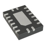 SN74AHC238BQBR

The activity of extra discounts on wholesale prices is in full swing…
Please fill in your contact information and we will send you the latest wholesale price list.







