 ChipApex | Global Electronic Components Supplier
SEARCH
Search Product
Search Post
— IC芯片 | 连接器 | 传感器 | 被动器件 —
Search productSearch post
— IC芯片 | 连接器 | 传感器 | 被动器件 —
Consult the customer manager about the wholesale price.
consultation hotline:86-132-6715-2157
email:[email protected]
Contact the product manager for consultation. One-stop consultation is available.
Do you want a lower wholesale price? Please send us your inquiry and we will reply immediately.
The SN74AHCT14PW is a commercial-grade hex Schmitt-trigger inverter from the AHCT logic family, housed in a 14-pin TSSOP package. It operates within a supply voltage range of 4.5 V to 5.5 V and supports an operating temperature range of -40°C to +125°C. The device features TTL-compatible inputs with distinct positive-going (VT+) and negative-going (VT-) threshold voltages to provide hysteresis. Electrical characteristics include a high-level output current of -8 mA and a low-level output current of 8 mA. Propagation delays are specified at 1 ns to 9 ns depending on load capacitance.
Verify the specific ordering suffix against the manufacturer's latest Package Option Addendum to confirm active production status and moisture sensitivity level ratings. Ensure the selected package variant matches the required thermal resistance values for the target application environment. Cross-reference the datasheet revision history to validate updated thermal metrics and parameter testing conditions before finalizing procurement specifications.
Select this component when TTL compatibility is required alongside noise filtering capabilities provided by Schmitt triggers. The AHCT series bridges the gap between CMOS performance and TTL input thresholds. Consider the TSSOP package dimensions and thermal characteristics relative to board space constraints. Verify that the operating temperature range meets the environmental requirements of the deployment location.
This device belongs to the SNx4AHCT14 family of hex inverters manufactured by Texas Instruments. The 'SN' prefix indicates a commercial rating, while '74' denotes the standard industrial temperature range. The 'AHCT' series specifies advanced high-speed CMOS technology with TTL-compatible inputs. This family includes various package options such as SOIC, SSOP, and VQFN to suit different PCB layout needs.
SN74AHCT14PWR
The Schmitt trigger provides different input threshold levels for positive-going and negative-going signals. This hysteresis prevents output oscillation caused by slow-rising or noisy input waveforms, effectively cleaning up the signal.
All unused inputs must be held at VCC or GND to ensure proper device operation. Floating inputs can result in undefined operational states and increased power consumption due to partial conduction of drive transistors.
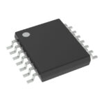 SN74AHCT14PW-P
The activity of extra discounts on wholesale prices is in full swing…
Please fill in your contact information and we will send you the latest wholesale price list.





