 ChipApex | Global Electronic Components Supplier

SEARCH
Search Product
Search Post
— IC芯片 | 连接器 | 传感器 | 被动器件 —
Search productSearch post
— IC芯片 | 连接器 | 传感器 | 被动器件 —
Consult the customer manager about the wholesale price.
consultation hotline:86-132-6715-2157
email:[email protected]
Contact the product manager for consultation. One-stop consultation is available.
Do you want a lower wholesale price? Please send us your inquiry and we will reply immediately.
SN74ALS166DBR is listed in the Shift Registers range at ChipApex. The manufacturer field lists Texas Instruments. Its product description is IC PAR-LOAD SHIFT REGIST 16-SSOP. Review the specifications below when checking this part for your BOM.
The SN74ALS166DBR is a parallel-load 8-bit shift register from the Texas Instruments ALS logic family. It operates within a supply voltage range of 4.5 V to 5.5 V and supports clock frequencies up to 45 MHz. The device features buffered inputs, input clamping diodes, and an overriding clear function. It is housed in a 16-pin Shrink Small-Outline (DB) package and is characterized for operation between 0°C and 70°C.
Verify the active status and RoHS compliance of the SN74ALS166DBR through official Texas Instruments channels before procurement. Confirm the specific SSOP-16 tape and reel packaging details match your assembly requirements. Ensure the operating temperature range aligns with your environmental specifications.
Select this component when a fast, low-power 8-bit shift register with parallel loading capability is required. The ALS series offers superior speed compared to standard TTL while maintaining lower power consumption. Verify compatibility with existing logic families and ensure the 16-pin SSOP footprint fits the PCB layout constraints.
This part belongs to the SN74ALS166A family of parallel-load 8-bit shift registers. It is designed for high-speed digital applications where efficient data serialization or deserialization is necessary. The device integrates buffered inputs and clamping diodes to simplify system design and minimize switching transients.
Check for direct substitutes such as the SN74ALS166DR or SN74ALS166N based on package preference. Verify functional equivalence regarding pinout and electrical characteristics before replacing the DB package variant.
When SH/LD is high, the register accepts serial data at the SER input. When SH/LD is low, parallel data from inputs A through H is loaded synchronously on the next clock pulse.
The CLK INH input allows the system clock to be inhibited. Holding either the CLK or CLK INH input high prevents clocking, enabling the register to stop shifting on command.
Explore related parts through Logic, Integrated Circuits (ICs), all product categories, ChipApex homepage.
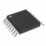 SN74ALS166DBR

The activity of extra discounts on wholesale prices is in full swing…
Please fill in your contact information and we will send you the latest wholesale price list.





