 ChipApex | Global Electronic Components Supplier

SEARCH
Search Product
Search Post
— IC芯片 | 连接器 | 传感器 | 被动器件 —
Search productSearch post
— IC芯片 | 连接器 | 传感器 | 被动器件 —
Consult the customer manager about the wholesale price.
consultation hotline:86-132-6715-2157
email:[email protected]
Contact the product manager for consultation. One-stop consultation is available.
Do you want a lower wholesale price? Please send us your inquiry and we will reply immediately.
SN74ALS166DR is listed in the Shift Registers range at ChipApex. The manufacturer field lists Texas Instruments. Its product description is IC SHIFT REG 8BIT PARALL 16-SOIC. Review the specifications below when checking this part for your BOM.
The SN74ALS166DR is a parallel-load 8-bit shift register from the ALS logic family, housed in a 16-pin SOIC package. It operates within a supply voltage range of 4.5 V to 5.5 V and supports an operating temperature range of 0°C to 70°C. The device features a maximum clock frequency of 45 MHz, with propagation delays ranging from 2 ns to 14 ns depending on the signal path. It includes asynchronous clear, gated clock inputs, and input clamping diodes for transient suppression.
Verify the specific ordering suffix 'DR' corresponds to the SOIC package and tape-and-reel quantity of 2500 units. Confirm RoHS compliance status and lead finish details against the latest Package Option Addendum. Ensure the component meets the specified commercial temperature range of 0°C to 70°C for your application environment.
Select this component when designing with the ALS logic family for its speed and power characteristics. Ensure the system operates strictly within the 4.5 V to 5.5 V supply voltage limits. Verify that the required clock frequency does not exceed the 45 MHz maximum rating. Consider the 16-pin SOIC footprint constraints during PCB layout.
This part belongs to the SN74ALS166 series of parallel-load 8-bit shift registers. It is compatible with most other TTL logic families. The 'DR' suffix specifically denotes the plastic small-outline (D) package configuration. It serves as a digital storage element for sequential logic applications requiring serial data handling.
Compatible substitutes include SN74ALS166N (PDIP), SN74ALS166DBR (SSOP), and SN74ALS166NSR (SOP). These variants share identical electrical specifications and pinouts but differ in physical package dimensions and reel quantities.
The mode is established by the SH/LD input. When high, the device shifts serial data; when low, it synchronously loads parallel data on the next clock pulse.
The CLK INH input acts as a clock inhibit. Holding either clock input high inhibits clocking, while holding it low enables the other clock input.
Explore related parts through Logic, Integrated Circuits (ICs), all product categories, ChipApex homepage.
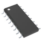 SN74ALS166DR

The activity of extra discounts on wholesale prices is in full swing…
Please fill in your contact information and we will send you the latest wholesale price list.





