 ChipApex | Global Electronic Components Supplier
SEARCH
Search Product
Search Post
— IC芯片 | 连接器 | 传感器 | 被动器件 —
Search productSearch post
— IC芯片 | 连接器 | 传感器 | 被动器件 —
Consult the customer manager about the wholesale price.
consultation hotline:86-132-6715-2157
email:[email protected]
Contact the product manager for consultation. One-stop consultation is available.
Do you want a lower wholesale price? Please send us your inquiry and we will reply immediately.
The SN74ALVC08IPWRQ1 is a quadruple 2-input positive-AND gate designed for automotive applications. It operates from a supply voltage range of 1.65 V to 3.6 V and features a maximum propagation delay of 2.9 ns at 3.3 V. The device provides ±24-mA output drive capability at 3.3 V and includes ESD protection exceeding 2000 V per MIL-STD-883, Method 3015. Latch-up performance exceeds 250 mA per JESD 17. It is housed in a TSSOP (PW) package with 14 pins.
Verify the specific ordering suffix 'IPWRQ1' corresponds to the TSSOP-14 package and -40°C to 85°C operating temperature range. Confirm RoHS compliance and lead finish details via the latest Package Option Addendum. Ensure the component meets the required automotive qualification standards before integration into production designs.
Select this component when automotive-grade reliability and high-speed AND logic are required within a 1.65-V to 3.6-V supply range. Consider the TSSOP-14 package constraints and thermal impedance characteristics. Verify input transition rates do not exceed specified limits to maintain timing accuracy.
This part belongs to the SN74ALVC08-Q1 family of quadruple 2-input positive-AND gates. It is an automotive-qualified version of the standard SN74ALVC08 series, offering enhanced reliability for harsh environments while maintaining compatibility with low-voltage digital logic interfaces.
SN74ALVC08IDRQ1 (SOIC-14 package)
The maximum propagation delay is 2.9 ns at a supply voltage of 3.3 V.
Yes, the device is qualified for automotive applications.
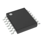 SN74ALVC08IPWRQ1
The activity of extra discounts on wholesale prices is in full swing…
Please fill in your contact information and we will send you the latest wholesale price list.





