 ChipApex | Global Electronic Components Supplier

SEARCH
Search Product
Search Post
— IC芯片 | 连接器 | 传感器 | 被动器件 —
Search productSearch post
— IC芯片 | 连接器 | 传感器 | 被动器件 —
Consult the customer manager about the wholesale price.
consultation hotline:86-132-6715-2157
email:[email protected]
Contact the product manager for consultation. One-stop consultation is available.
Do you want a lower wholesale price? Please send us your inquiry and we will reply immediately.
SN74ALVC16244AZRDR is listed in the Buffers, Drivers, Receivers, Transceivers range at ChipApex. The manufacturer field lists Texas Instruments. Its product description is IC BUFFER NON-INVERT 3.6V 54BGA. Review the specifications below when checking this part for your BOM.
The SN74ALVC16244AZRDR is a 16-bit buffer and driver with 3-state outputs from the Texas Instruments Widebus family. It operates within a supply voltage range of 1.65 V to 3.6 V. The device provides symmetrical active-low output-enable inputs and true outputs, designed for memory-address drivers, clock drivers, and bus-oriented receivers. It features a maximum propagation delay of 3 ns at 3.3 V and supports ±24-mA output drive current at 3.3 V. The component includes ESD protection exceeding JESD 22 standards.
Verify the specific ordering suffix 'ZRDR' corresponds to the required package type and lead finish before procurement. Confirm that the Pb-free designation aligns with project environmental compliance requirements. Ensure the operating temperature range of -40 °C to 85 °C meets the application's thermal specifications. Cross-reference the datasheet revision date to ensure compatibility with existing design documentation.
Select this component when a 16-bit wide data path requires high-speed buffering with low power consumption in the ALVC series. It is suitable for applications needing operation down to 1.65 V. Consider the 3 ns propagation delay for timing-critical designs. Verify that the 3-state output configuration matches the bus architecture requirements. Evaluate the package options if space constraints differ from the standard reel packaging.
This part belongs to the SN74ALVC16244A family, which includes variants like SN74ALVC16244ADGGR and SN74ALVC16244ADLR. These devices share the same core logic function but differ in package types such as TSSOP, SSOP, and FBGA. The family is characterized by its ability to operate across a wide voltage range while maintaining fast switching speeds.
SN74ALVC16244ADGGR
To ensure the high-impedance state during power up or power down, OE should be tied to VCC through a pullup resistor.
The maximum propagation delay is 3 ns at 3.3 V.
Explore related parts through Logic, Integrated Circuits (ICs), all product categories, ChipApex homepage.
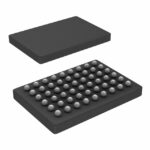 SN74ALVC16244AZRDR

The activity of extra discounts on wholesale prices is in full swing…
Please fill in your contact information and we will send you the latest wholesale price list.





