 ChipApex | Global Electronic Components Supplier
SEARCH
Search Product
Search Post
— IC芯片 | 连接器 | 传感器 | 被动器件 —
Search productSearch post
— IC芯片 | 连接器 | 传感器 | 被动器件 —
Consult the customer manager about the wholesale price.
consultation hotline:86-132-6715-2157
email:[email protected]
Contact the product manager for consultation. One-stop consultation is available.
Do you want a lower wholesale price? Please send us your inquiry and we will reply immediately.
The SN74ALVC7803 is a 512 × 18 clocked first-in, first-out memory device designed for 3-V to 3.6-V VCC operation. It supports data rates from 0 to 50 MHz with fast access times of 13 ns under a 50-pF load and simultaneous switching conditions. The component features independent read and write clocks that can be asynchronous or coincident. It includes programmable almost-full/almost-empty flags, half-full flag, input-ready, and output-ready status indicators. The device is housed in a 56-pin shrink small-outline (DL) package.
Verify the specific suffix DL indicates the 56-pin shrink small-outline package with 25-mil lead spacing. Confirm the operating temperature range matches the application requirements, as standard versions typically cover 0°C to 70°C. Ensure supply voltage constraints between 3 V and 3.6 V are strictly maintained during system design and validation.
Select this component when a 512-word by 18-bit depth is required for synchronous data buffering. It is suitable for systems needing independent read and write clock domains. Consider its pin compatibility with SN74ACT7803 if migrating from older ACT logic families. Evaluate power dissipation calculations based on clock frequency and load capacitance for thermal management.
This device belongs to the SN74ALVC78xx series of advanced low-voltage CMOS FIFO memories. It utilizes Texas Instruments' low-power advanced CMOS technology. The part is functionally compatible with previous generation ACT logic but operates at lower voltages. It serves as a specialized memory buffer for high-speed digital signal processing and communication interfaces.
SN74ACT7803 is documented as pin-compatible.
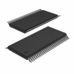 SN74ALVC7803-25DL
The activity of extra discounts on wholesale prices is in full swing…
Please fill in your contact information and we will send you the latest wholesale price list.





