 ChipApex | Global Electronic Components Supplier
SEARCH
Search Product
Search Post
— IC芯片 | 连接器 | 传感器 | 被动器件 —
Search productSearch post
— IC芯片 | 连接器 | 传感器 | 被动器件 —
Consult the customer manager about the wholesale price.
consultation hotline:86-132-6715-2157
email:[email protected]
Contact the product manager for consultation. One-stop consultation is available.
Do you want a lower wholesale price? Please send us your inquiry and we will reply immediately.
The SN74ALVCH16903DGVR is a 3.3-V, 12-bit universal bus driver with parity checker and dual 3-state outputs from the Texas Instruments Widebus family. It operates on a 2.3-V to 3.6-V supply voltage range within an operating temperature of 0°C to 70°C. The device features active bus-hold circuitry on data inputs, eliminating the need for external pullup or pulldown resistors. It supports edge-triggered register mode and buffer mode via the MODE input, with clock enable (CLKEN) control. Parity checking occurs on APAR one cycle after data arrival, producing an open-drain YERR output. The DGV package provides a thin very small-outline form factor.
Verify the specific DGVR suffix indicates the Thin Very Small-Outline (DGV) package variant when sourcing. Confirm the operating temperature range aligns with your system requirements, as this part is characterized for 0°C to 70°C. Ensure power supply voltages remain strictly within the 2.3-V to 3.6-V limits to prevent damage. Check for any recent Product Change Notifications regarding assembly or material updates before finalizing procurement.
Select this component when designing 3.3-V bus architectures that require integrated parity checking and dual output paths. It is suitable for applications needing active bus-hold to simplify interface design by removing external resistors. Consider the DGV package constraints if board space is limited. Ensure the system can accommodate the specific setup and hold times required for register mode operation at the target clock frequency.
This device belongs to the Texas Instruments ALVCH logic series, designed for low-voltage CMOS applications. It is part of the Widebus family, which emphasizes high-density bus driving capabilities. The SN74ALVCH16903 specifically addresses the need for parity integrity in 12-bit wide data buses, combining buffering, latching, and error detection in a single package.
Public confirmed substitute part numbers: SN74ALVCH16903DL, SN74ALVCH16903DL.B.
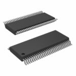 SN74ALVCH16903DGVR
The activity of extra discounts on wholesale prices is in full swing…
Please fill in your contact information and we will send you the latest wholesale price list.





