 ChipApex | Global Electronic Components Supplier

SEARCH
Search Product
Search Post
— IC芯片 | 连接器 | 传感器 | 被动器件 —
Search productSearch post
— IC芯片 | 连接器 | 传感器 | 被动器件 —
Consult the customer manager about the wholesale price.
consultation hotline:86-132-6715-2157
email:[email protected]
Contact the product manager for consultation. One-stop consultation is available.
Do you want a lower wholesale price? Please send us your inquiry and we will reply immediately.
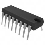
The SN74AS298AN is a quadruple 2-input multiplexer with storage, combining the functionality of two MSI functions in a single 16-pin package. It selects between two 4-bit data sources and synchronously stores data on the negative-going edge of the clock pulse. The device operates within a supply voltage range of 4.5 V to 5.5 V and supports a maximum clock frequency of 62 MHz. Propagation delays from CLK to Q range from 1 ns to 11 ns. It features TTL inputs and outputs, with low-level output current capability of 20 mA.
Verify the specific ordering suffix to confirm the package type, as the SN74AS298A series includes both SOIC (D) and PDIP (N) options. Ensure the required operating temperature range aligns with the commercial specification of 0°C to 70°C. Confirm RoHS compliance status and lead finish details against the latest manufacturer packaging addendum before finalizing procurement specifications.
Select this component when design requirements necessitate combining multiplexing and latching functions to reduce component count. It serves as an equivalent functional replacement for using separate SN74AS157 and SN74AS175A devices. Consider the 16-pin package constraint and ensure the system clock frequency does not exceed the specified maximum limit for reliable operation.
This part belongs to the Texas Instruments SN74AS logic family, known for high-speed performance compared to standard TTL. The 'AN' suffix specifically denotes the plastic DIP package variant. It is designed for applications requiring fast data selection and storage within digital systems, offering a compact solution for complex logic routing tasks.
SN74AS298AD
 SN74AS298AN

The activity of extra discounts on wholesale prices is in full swing…
Please fill in your contact information and we will send you the latest wholesale price list.





