 ChipApex | Global Electronic Components Supplier
SEARCH
Search Product
Search Post
— IC芯片 | 连接器 | 传感器 | 被动器件 —
Search productSearch post
— IC芯片 | 连接器 | 传感器 | 被动器件 —
Consult the customer manager about the wholesale price.
consultation hotline:86-132-6715-2157
email:[email protected]
Contact the product manager for consultation. One-stop consultation is available.
Do you want a lower wholesale price? Please send us your inquiry and we will reply immediately.
The SN74AUC16501DGGR is an 18-bit universal bus transceiver from the Widebus family, designed for sub-1-V operation with a supply voltage range of 0.8 V to 2.7 V. It features Ioff support for partial-power-down mode and is optimized for 1.8-V operation while remaining 3.6-V I/O tolerant. The device provides data flow control via output-enable, latch-enable, and clock inputs, supporting both transparent and latched modes. It operates within a temperature range of -40°C to 85°C and utilizes a 56-pin TSSOP package.
Verify the specific ordering suffix DGGR corresponds to the tape and reel packaging format required for your assembly line. Confirm that the component meets RoHS compliance standards applicable to your region. Ensure that all unused inputs are properly terminated to VCC or GND during operation to maintain device functionality and stability.
Select this component when designing systems requiring wide voltage compatibility between 0.8 V and 2.7 V. It is suitable for applications needing robust ESD protection and low power consumption. Consider its 18-bit width for high-density data bus interfaces where space efficiency is critical.
This device belongs to Texas Instruments' Widebus family, which focuses on high-density bus solutions. It complements other logic families by offering specialized low-voltage operation capabilities. The SN74AUC16501 series is engineered to bridge different voltage domains efficiently.
SN74AUC16501DGV
The integrated Ioff circuitry automatically disables the outputs when the device is powered down, preventing current backflow through the part.
Data flow is managed by complementary output-enable (OEAB and OEBA) signals, along with latch-enable and clock inputs for each direction.
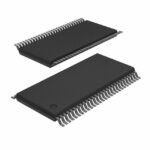 SN74AUC16501DGGR
The activity of extra discounts on wholesale prices is in full swing…
Please fill in your contact information and we will send you the latest wholesale price list.





