 ChipApex | Global Electronic Components Supplier
SEARCH
Search Product
Search Post
— IC芯片 | 连接器 | 传感器 | 被动器件 —
Search productSearch post
— IC芯片 | 连接器 | 传感器 | 被动器件 —
Consult the customer manager about the wholesale price.
consultation hotline:86-132-6715-2157
email:[email protected]
Contact the product manager for consultation. One-stop consultation is available.
Do you want a lower wholesale price? Please send us your inquiry and we will reply immediately.
The SN74AUC16501DGVR is an 18-bit universal bus transceiver from the Widebus family, designed for sub-1-V operation with a supply voltage range of 0.8 V to 2.7 V. It features 3-state outputs and supports mixed-mode signal operation through 3.6-V I/O tolerance. The device includes latch/flip-flop functionality controlled by OEAB, LEAB, and CLKAB inputs. It offers a maximum propagation delay of 2 ns at 1.8 V and low power consumption of 10 µA at 1.8 V. Packaged in a TVSOP-56 (DGV) format, it operates within a temperature range of -40°C to +85°C.
Verify the specific ordering suffix DGVR corresponds to the TVSOP-56 package configuration required for your design. Confirm that the component meets RoHS standards as indicated in manufacturer documentation. Ensure compatibility with your system's voltage levels, specifically the 0.8 V to 2.7 V operating range. Check for any recent product change notices regarding availability or pinout modifications before finalizing procurement plans.
Select this component when designing systems requiring 18-bit data transfer with integrated latching capabilities at sub-1-V logic levels. It is suitable for applications needing robust ESD protection and mixed-voltage interface support. Consider the TVSOP-56 package constraints for PCB layout. Evaluate the trade-off between the 2 ns propagation delay and power consumption against other Widebus family members if higher speed or lower voltage operation is required.
This device belongs to Texas Instruments' Widebus family, which specializes in high-density bus transceivers optimized for low-voltage operation. The SN74AUC16501 series provides universal bus functionality with configurable data flow directions. It complements other logic families by offering enhanced performance at reduced supply voltages while maintaining compatibility with standard 3.6-V tolerant interfaces.
SN74AUC16501DGGR is a direct replacement in the TSSOP-56 package. SN74AUC16501GQLR is available in the VFBGA package. Verify pinout compatibility and thermal requirements when substituting packages.
The device includes dedicated Ioff circuitry that automatically disables the outputs when powered down, preventing damaging current backflow through the device into the power supply.
All unused inputs must be held at VCC or GND to ensure proper device operation and prevent undefined states or excessive current consumption.
The output enables are complementary; OEAB is active high, while OEBA is active low, allowing independent control of data flow direction from A to B and B to A.
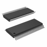 SN74AUC16501DGVR
The activity of extra discounts on wholesale prices is in full swing…
Please fill in your contact information and we will send you the latest wholesale price list.





