 ChipApex | Global Electronic Components Supplier
SEARCH
Search Product
Search Post
— IC芯片 | 连接器 | 传感器 | 被动器件 —
Search productSearch post
— IC芯片 | 连接器 | 传感器 | 被动器件 —
Consult the customer manager about the wholesale price.
consultation hotline:86-132-6715-2157
email:[email protected]
Contact the product manager for consultation. One-stop consultation is available.
Do you want a lower wholesale price? Please send us your inquiry and we will reply immediately.
The SN74AUC1G06DBVR is a single inverter buffer/driver with open-drain output from the Texas Instruments AUC logic family. It operates at supply voltages between 0.8 V and 2.7 V, optimized for 1.65-V to 1.95-V applications. The device features low power consumption with a maximum quiescent current of 10 μA and supports partial-power-down mode via Ioff circuitry. It provides an output drive of ±8 mA at 1.8 V and exhibits a maximum propagation delay of 2.5 ns at 1.8 V. Packaged in a five-pin SOT-23 (DBV) format, it ensures robust latch-up performance exceeding 100 mA per JESD 78 Class II standards.
Verify the specific ordering suffix 'DBVR' corresponds to the SOT-23 package with a 3000-unit large tape and reel quantity. Confirm that the component meets RoHS compliance standards and utilizes NIPDAU lead finish. Ensure the operating temperature range aligns with industrial requirements spanning -40°C to +85°C. Cross-reference the part marking 'U06R' for identification during assembly inspection.
Select this component when designing low-voltage systems requiring sub-1-V operation and minimal power consumption. The open-drain output necessitates an external pull-up resistor for high-level signaling. Consider the 2.5 ns propagation delay for timing-critical paths within the specified voltage window. Verify input transition rates against the recommended slew rate limits to ensure proper switching characteristics.
This device belongs to the SN74AUC1G06 series, representing Texas Instruments' NanoFree technology. It serves as a compact solution for space-constrained designs requiring single-gate inversion. The DBVR variant specifically denotes the surface-mount SOT-23 package configuration. It complements other AUC family members by providing high-speed performance at ultra-low supply voltages.
SN74AUC1G06DBVRE4: Equivalent production part with identical electrical specifications and packaging.
The Ioff circuitry disables outputs when the device is powered down, preventing damaging current backflow through the device during partial-power-down operations.
The input voltage can withstand up to 3.6 V, allowing the device to support mixed-mode signal operation even when powered by lower supply voltages.
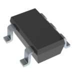 SN74AUC1G06DBVR
The activity of extra discounts on wholesale prices is in full swing…
Please fill in your contact information and we will send you the latest wholesale price list.





