 ChipApex | Global Electronic Components Supplier
SEARCH
Search Product
Search Post
— IC芯片 | 连接器 | 传感器 | 被动器件 —
Search productSearch post
— IC芯片 | 连接器 | 传感器 | 被动器件 —
Consult the customer manager about the wholesale price.
consultation hotline:86-132-6715-2157
email:[email protected]
Contact the product manager for consultation. One-stop consultation is available.
Do you want a lower wholesale price? Please send us your inquiry and we will reply immediately.
The SN74AUP1G00DSF2 is a single 2-input positive-NAND gate from Texas Instruments' AUP logic family, housed in a 6-pin SON (DSF) package. It operates within a supply voltage range of 0.8 V to 3.6 V and supports an operating temperature from -40°C to +85°C. The device features low static power consumption with a maximum ICC of 0.9 µA and typical dynamic power dissipation capacitance of 4 pF at 3.3 V. Propagation delay reaches a maximum of 4.8 ns at 3.3 V with a 5 pF load. Input hysteresis is typically 250 mV at 3.3 V, and the I/Os are tolerant up to 3.6 V.
Verify the specific DSF package variant against the orderable addendum in the datasheet to ensure correct pinout and mechanical dimensions. Confirm that the application environment remains within the specified -40°C to +85°C operating temperature range. Ensure unused inputs are tied to VCC or GND to prevent floating states and excessive current draw. Check ESD handling requirements during assembly.
Select this component for designs requiring minimal board space and ultra-low power in portable electronics. The 3.6-V I/O tolerance allows compatibility with mixed-mode signal operations involving 3.3-V systems. Consider the propagation delay specifications relative to the system clock speed and load capacitance requirements. Verify that the output drive capabilities meet the downstream input requirements without exceeding the 20 mA continuous output current limit.
This device belongs to the SN74AUP1Gxx series, representing Texas Instruments' ultra-low power single-gate logic solutions. The AUP family utilizes advanced CMOS technology to achieve sub-microampere static currents while maintaining high-speed performance. The DSF package offers a compact footprint compared to traditional SOT-23 or SC70 options, facilitating dense PCB layouts for modern handheld and wearable devices.
SN74AUP1G00DBV
The Ioff circuitry disables the outputs when VCC is 0 V, preventing damaging current backflow through the device. This supports partial-power-down modes and live insertion.
Input hysteresis allows for slower input transition rates and provides better switching noise immunity at the input pins, ensuring stable operation in noisy environments.
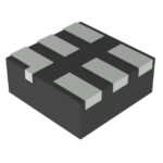 SN74AUP1G00DSF2
The activity of extra discounts on wholesale prices is in full swing…
Please fill in your contact information and we will send you the latest wholesale price list.





