 ChipApex | Global Electronic Components Supplier
SEARCH
Search Product
Search Post
— IC芯片 | 连接器 | 传感器 | 被动器件 —
Search productSearch post
— IC芯片 | 连接器 | 传感器 | 被动器件 —
Consult the customer manager about the wholesale price.
consultation hotline:86-132-6715-2157
email:[email protected]
Contact the product manager for consultation. One-stop consultation is available.
Do you want a lower wholesale price? Please send us your inquiry and we will reply immediately.
The SN74AUP1G02DRLR is a single 2-input positive-NOR gate from the Texas Instruments AUP family. It operates within a supply voltage range of 0.8 V to 3.6 V and supports an operating temperature range of -40°C to +85°C. The device features low static power consumption with a maximum ICC of 0.9 μA and low dynamic power consumption characterized by a typical Cpd of 4.3 pF at 3.3 V. Propagation delay (tpd) is typically 2.4 ns at 3.3 V with a 5 pF load, reaching a maximum of 4.6 ns under the same conditions. Input hysteresis is typically 250 mV at 3.3 V.
Verify that the ordering suffix DRLR corresponds to the specific SOT package variant required for your design. Confirm the RoHS compliance status and lead finish details against the manufacturer's current orderable addendum. Ensure the component meets the specified thermal resistance requirements for your PCB layout. Check for any recent documentation updates or revision history changes that may affect pinout or electrical characteristics before finalizing procurement.
Select this component when designing systems requiring ultra-low power consumption across a wide voltage range of 0.8 V to 3.6 V. It is suitable for translating signals between 3.3 V peripherals and lower voltage microprocessors. Consider its Ioff feature if the application involves hot-swapping or partial power-down scenarios. Verify that the propagation delay specifications meet the timing requirements of your specific digital logic interface.
This device belongs to the SN74AUP1Gxx series of single-function gates manufactured by Texas Instruments. The AUP family is designed specifically for low-power applications, offering reduced quiescent current compared to standard CMOS families. It utilizes advanced packaging technologies to minimize physical size while maintaining reliable performance in consumer electronics and portable devices.
SN74AUP1G02DBVR
It performs the single 2-input positive-NOR gate function, represented as Y = A + B or Y = A × B in positive logic.
The Ioff circuitry disables outputs when VCC is 0 V, preventing damaging current backflow through the device and supporting live insertion capabilities.
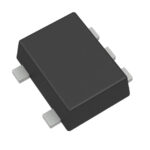 SN74AUP1G02DRLR
The activity of extra discounts on wholesale prices is in full swing…
Please fill in your contact information and we will send you the latest wholesale price list.





