 ChipApex | Global Electronic Components Supplier
SEARCH
Search Product
Search Post
— IC芯片 | 连接器 | 传感器 | 被动器件 —
Search productSearch post
— IC芯片 | 连接器 | 传感器 | 被动器件 —
Consult the customer manager about the wholesale price.
consultation hotline:86-132-6715-2157
email:[email protected]
Contact the product manager for consultation. One-stop consultation is available.
Do you want a lower wholesale price? Please send us your inquiry and we will reply immediately.
The SN74AUP3G04RSER is a low-power triple inverter gate from the Texas Instruments AUP logic family. It operates within a supply voltage range of 0.8 V to 3.6 V and features I/O tolerance up to 3.6 V, supporting mixed-mode operations. The device is housed in an 8-pin UQFN (1.5x1.5 mm) package. Key electrical parameters include a maximum propagation delay of 6.2 ns at 3.3 V with 30 pF load, static current of 500 nA, and an operating temperature range of -40°C to +85°C.
Verify the specific suffix RSER corresponds to the UQFN-8 package and tape-and-reel shipping configuration. Confirm RoHS compliance status through official manufacturer documentation prior to integration. Ensure input voltage levels remain within the specified 0.8-V to 3.6-V operational window to maintain signal integrity and prevent device damage during operation.
Select this component when minimizing power consumption is critical alongside maintaining compatibility with 3.6-V systems. The UQFN package offers a small footprint suitable for dense PCB designs. Compare propagation delay specifications against system timing requirements to ensure adequate performance margins for high-speed digital signaling applications.
This part belongs to the SN74AUP3Gxx series of triple logic gates. The AUP family provides superior speed-to-power efficiency compared to older CMOS technologies. The '04' designation indicates inverter functionality, while '3G' specifies three independent channels within a single compact integrated circuit package.
Direct substitutes include other SN74AUP3G04 variants such as SN74AUP3G04DCUR or SN74AUP3G04RSER.B, provided pinout and package dimensions match. Verify that alternative packages maintain identical electrical characteristics and thermal performance for seamless integration.
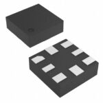 SN74AUP3G04RSER
The activity of extra discounts on wholesale prices is in full swing…
Please fill in your contact information and we will send you the latest wholesale price list.





