 ChipApex | Global Electronic Components Supplier
SEARCH
Search Product
Search Post
— IC芯片 | 连接器 | 传感器 | 被动器件 —
Search productSearch post
— IC芯片 | 连接器 | 传感器 | 被动器件 —
Consult the customer manager about the wholesale price.
consultation hotline:86-132-6715-2157
email:[email protected]
Contact the product manager for consultation. One-stop consultation is available.
Do you want a lower wholesale price? Please send us your inquiry and we will reply immediately.
The SN74BCT29843DW is a nine-bit D-type latch with three-state outputs manufactured by Texas Instruments. It utilizes a BiCMOS process featuring CMOS inputs and TTL outputs to reduce standby current. The device operates within a supply voltage range of 4.5 V to 5.5 V and supports an operating temperature range of 0°C to 70°C. Key electrical characteristics include a high-level output current of -24 mA and a low-level output current of 48 mA at VCC = 5 V. Propagation delays from data input (D) to output (Q) are typically 4.5 ns for low-to-high and 5.7 ns for high-to-low transitions under a 50 pF load.
Verify the specific package variant during procurement, as the DW suffix denotes a plastic small-outline package. Confirm RoHS compliance status, noting that E4 and G4 suffixes indicate lead-free and green material classifications respectively. Ensure the active status aligns with design requirements, as TI recommends this device for new designs. Cross-reference the pinout diagram for the 24-pin configuration to ensure compatibility with the target PCB footprint.
Select this component when designing systems requiring nine-bit storage with high-drive three-state outputs. The BiCMOS technology offers a balance of CMOS input compatibility and TTL output drive strength. Consider the propagation delay specifications if timing constraints are critical for the bus interface. Verify that the operating temperature range meets the environmental conditions of the final application.
This device belongs to the SN74BCT series, which combines BiCMOS processing with CMOS inputs and TTL outputs. The family is designed to provide improved performance over standard TTL logic while maintaining compatibility. The SN74BCT29843 specifically addresses applications needing wide bus interfacing with reduced power consumption compared to older bipolar technologies.
SN74BCT29843DWE4
The output-enable input does not affect the internal operation of the flip-flops. Data can be retained or entered while the outputs are in the high-impedance state.
When the latch-enable input is high, the Q outputs are complementary to the noninverting data inputs.
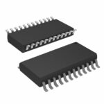 SN74BCT29843DW
The activity of extra discounts on wholesale prices is in full swing…
Please fill in your contact information and we will send you the latest wholesale price list.





