 ChipApex | Global Electronic Components Supplier
SEARCH
Search Product
Search Post
— IC芯片 | 连接器 | 传感器 | 被动器件 —
Search productSearch post
— IC芯片 | 连接器 | 传感器 | 被动器件 —
Consult the customer manager about the wholesale price.
consultation hotline:86-132-6715-2157
email:[email protected]
Contact the product manager for consultation. One-stop consultation is available.
Do you want a lower wholesale price? Please send us your inquiry and we will reply immediately.
The SN74BCT29843NT is a nine-bit latch with three-state outputs manufactured by Texas Instruments. It utilizes a BiCMOS process featuring CMOS inputs and TTL outputs to reduce standby current. The device operates within a supply voltage range of 4.5 V to 5.5 V and supports an operating temperature range of 0°C to 70°C. Key electrical characteristics include a high-level output current of -24 mA and a low-level output current of 48 mA at VCC = 5 V. Propagation delays from D to Q range from 1.5 ns to 9 ns, while OE-to-Q transitions vary between 2 ns and 15 ns depending on the direction.
Verify the package type matches the required design constraints, as the NT suffix denotes a standard plastic 300-mil DIP package. Confirm RoHS compliance status and lead finish specifications against current manufacturing updates. Ensure the operating environment remains within the specified 0°C to 70°C temperature range for optimal performance. Cross-reference the latest datasheet revision to confirm pinout consistency and electrical parameter tolerances before finalizing procurement orders.
Select this component when designing circuits requiring nine-bit storage with high-drive capability for bus applications. The BiCMOS technology offers a balance of speed and low power consumption suitable for general-purpose logic. Consider the PDIP package availability if through-hole mounting is necessary for prototyping or specific mechanical requirements. Evaluate the propagation delay specifications against system timing budgets to ensure signal integrity across the nine channels.
This device belongs to the SN74BCT series, which combines the speed of bipolar transistors with the low power consumption of CMOS technology. The BCT family is specifically engineered for high-performance digital applications requiring fast switching speeds and robust drive currents. The SN74BCT29843 variant focuses on latching functionality with three-state control, distinguishing it from simple buffers or inverters within the same logical family.
SN74BCT29843DW
The OE input controls only the external three-state outputs. It does not affect the internal operation of the flip-flops, allowing old data to be retained or new data to be entered while the outputs are in the high-impedance state.
The preset (PRE) and clear (CLR) inputs allow asynchronous forcing of the latch outputs. When active, they override the data inputs and latch-enable signal to set or reset the Q outputs to specific logic levels.
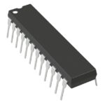 SN74BCT29843NT
The activity of extra discounts on wholesale prices is in full swing…
Please fill in your contact information and we will send you the latest wholesale price list.






