 ChipApex | Global Electronic Components Supplier

SEARCH
Search Product
Search Post
— IC芯片 | 连接器 | 传感器 | 被动器件 —
Search productSearch post
— IC芯片 | 连接器 | 传感器 | 被动器件 —
Consult the customer manager about the wholesale price.
consultation hotline:86-132-6715-2157
email:[email protected]
Contact the product manager for consultation. One-stop consultation is available.
Do you want a lower wholesale price? Please send us your inquiry and we will reply immediately.
The SN74CB3Q16211DGGR is a high-bandwidth FET bus switch from the Widebus family, organized as two 12-bit switches or one 24-bit switch. It operates on a single supply voltage ranging from 2.3 V to 3.6 V. The device features low and flat ON-state resistance with a typical value of 5 Ω. Data I/O ports support rail-to-rail switching for 0-V to 5-V signaling levels. Control inputs are compatible with TTL or 5-V/3.3-V CMOS outputs. The package is a 56-pin TSSOP.
Verify the specific ordering suffix 'DGGR' corresponds to the 56-pin TSSOP package in large tape-and-reel format (SPQ 2000). Confirm the component status is Active Production. Ensure the design accounts for the 2.3 V to 3.6 V supply range and check for RoHS compliance and lead finish specifications in the latest Package Option Addendum.
Select this component for broadband communications, networking, and data-intensive computing systems requiring optimized interfaces. It is suitable for applications needing PCI interface support, differential signal interfacing, memory interleaving, and bus isolation. The device handles both digital and analog applications effectively due to its low-distortion signal gating capabilities.
This part belongs to the Texas Instruments CB3Q series, designed for automotive and industrial reliability. It is functionally related to other Widebus family members like the SN74CBT16211A but offers enhanced performance characteristics including higher bandwidth and lower power consumption. The DGGR suffix specifically denotes the TSSOP package variant intended for surface-mount assembly.
Direct substitutes include SN74CB3Q16211DGVR (TVSOP package) and SN74CB3Q16211DLR (SSOP package). Verify pin compatibility and package dimensions before substitution.
The SN74CB3Q16211 includes Ioff circuitry that prevents damaging current backflow through the device when it is powered down, allowing safe operation in partial-power-down modes.
The maximum switching frequency for the OE control input is 20 MHz, measured under conditions where VO > VCC, VI = 5 V, RL ≥ 1 MΩ, and CL = 0.
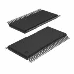 SN74CB3Q16211DGGR

The activity of extra discounts on wholesale prices is in full swing…
Please fill in your contact information and we will send you the latest wholesale price list.






