 ChipApex | Global Electronic Components Supplier

SEARCH
Search Product
Search Post
— IC芯片 | 连接器 | 传感器 | 被动器件 —
Search productSearch post
— IC芯片 | 连接器 | 传感器 | 被动器件 —
Consult the customer manager about the wholesale price.
consultation hotline:86-132-6715-2157
email:[email protected]
Contact the product manager for consultation. One-stop consultation is available.
Do you want a lower wholesale price? Please send us your inquiry and we will reply immediately.
The SN74CB3Q16211GQLR is a high-bandwidth FET bus switch from the Widebus family, packaged in a VFBGA (GQL) with 56 terminals. It operates on a single supply voltage ranging from 2.3 V to 3.6 V and supports data I/O voltages up to 5.5 V. The device contains two independent 12-bit bus switches, functioning as either two 12-bit or one 24-bit switch. It features a typical ON-state resistance of 5 Ω and low input/output capacitance of 4 pF when off.
Verify the GQL package designation matches the required footprint. Confirm that the 2.3 V to 3.6 V supply range aligns with system power rails. Ensure control inputs are pulled to VCC or GND to maintain proper operation. Check for RoHS compliance requirements if applicable to the manufacturing process.
Select this component for applications requiring high bandwidth and minimal signal distortion. The integrated charge pump ensures consistent performance over varying load conditions. Verify that the 56-terminal VFBGA package fits the available board space. Consider the 5-V tolerant I/O capability if interfacing with legacy logic levels.
This part belongs to Texas Instruments' Widebus family, designed for broadband communications and data-intensive computing. It serves as an optimized interface solution for networking equipment. The device replaces older bus switch technologies by offering superior speed and lower power consumption while maintaining compatibility with standard digital logic families.
SN74CB3Q16211DGGR
The SN74CB3Q16211GQLR includes Ioff circuitry that prevents damaging current backflow through the device when it is powered down but connected to active buses.
The maximum switching frequency for the OE control inputs is specified at 20 MHz under recommended operating conditions.
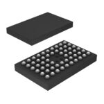 SN74CB3Q16211GQLR

The activity of extra discounts on wholesale prices is in full swing…
Please fill in your contact information and we will send you the latest wholesale price list.






