 ChipApex | Global Electronic Components Supplier

SEARCH
Search Product
Search Post
— IC芯片 | 连接器 | 传感器 | 被动器件 —
Search productSearch post
— IC芯片 | 连接器 | 传感器 | 被动器件 —
Consult the customer manager about the wholesale price.
consultation hotline:86-132-6715-2157
email:[email protected]
Contact the product manager for consultation. One-stop consultation is available.
Do you want a lower wholesale price? Please send us your inquiry and we will reply immediately.
The SN74CB3Q16811 is a 24-bit low-voltage FET bus switch featuring precharged outputs, designed for 2.5-V and 3.3-V systems with an operating range of 2.3 V to 3.6 V. It supports 0- to 5-V signaling levels on data I/Os and includes undershoot clamp diodes. The device utilizes a charge pump to maintain low ON-state resistance (r_on) of 5 Ω typical, enabling rail-to-rail switching. Key electrical parameters include a maximum switching frequency of 20 MHz, input capacitance of 3.5 pF typical, and output capacitance of 4 pF typical when off. It operates within a temperature range of -40°C to 85°C.
Verify the specific package variant required, as the SN74CB3Q16811DGGR denotes the TSSOP (DGG) package in tape and reel format. Confirm that the BIASV pin connection matches the active bus input threshold voltage to ensure effective glitch reduction during insertion events. Ensure control inputs are tied to VCC or GND to maintain proper high-impedance states during power transitions.
Select this component for high-bandwidth applications requiring minimal loading and flat ON-state resistance across the full voltage swing. It is suitable for broadband communications and data-intensive computing where signal integrity is critical. The device is equivalent to IDTQS3VH bus switches, allowing for potential direct replacements in designs utilizing that family. Consider the 56-pin TSSOP or TVSOP packages based on board space constraints.
This part belongs to the Texas Instruments Widebus family of bus switches. It is organized as two independent 12-bit bus switches, which can function as separate 12-bit units or combine into a single 24-bit switch. The device features separate output-enable inputs (1OE, 2OE) for controlling each 12-bit section independently, providing flexible configuration options for complex bus architectures.
The datasheet explicitly states that SN74CB3Q bus switches are equivalent to IDTQS3VH bus switches. Designers may consider IDTQS3VH variants as functional substitutes if pin compatibility and electrical specifications align with the system requirements.
The B-port outputs are precharged to the BIASV voltage through an equivalent 10-kΩ resistor when the switch is off or powered down. This ensures that insertion glitches do not cross the input threshold region of receivers, minimizing noise effects.
The I_off circuitry supports partial-power-down mode by preventing damaging current backflow through the device when it is powered down but connected to a live bus.
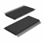 SN74CB3Q16811DGGR

The activity of extra discounts on wholesale prices is in full swing…
Please fill in your contact information and we will send you the latest wholesale price list.





