 ChipApex | Global Electronic Components Supplier

SEARCH
Search Product
Search Post
— IC芯片 | 连接器 | 传感器 | 被动器件 —
Search productSearch post
— IC芯片 | 连接器 | 传感器 | 被动器件 —
Consult the customer manager about the wholesale price.
consultation hotline:86-132-6715-2157
email:[email protected]
Contact the product manager for consultation. One-stop consultation is available.
Do you want a lower wholesale price? Please send us your inquiry and we will reply immediately.
The SN74CB3Q16811DL is a 24-bit FET bus switch from the Widebus family, organized as two independent 12-bit switches. It operates within a supply voltage range of 2.3 V to 3.6 V and supports data I/O levels from 0 V to 5.5 V. The device features low on-state resistance (typical 5 Ω) and utilizes a charge pump for gate elevation. B-port outputs are precharged via a bias voltage (BIASV) to minimize signal distortion during live insertion. It includes Ioff support for partial-power-down modes and undershoot clamp diodes on control inputs.
Verify the DL suffix corresponds to the SSOP package configuration before procurement. Confirm that the specific revision level matches the design requirements. Ensure the ordering quantity aligns with standard tube packaging specifications provided by the manufacturer. Cross-reference the part number against the latest availability status to confirm production readiness.
Select this component for high-bandwidth interfaces requiring rail-to-rail switching capabilities. The integrated charge pump ensures flat on-state resistance across the operating voltage range. Consider the separate output-enable inputs for managing distinct 12-bit segments independently. Evaluate the thermal impedance characteristics relative to the system's heat dissipation constraints.
This device belongs to the Texas Instruments Widebus family of low-voltage FET bus switches. It is designed to provide optimized interface solutions for broadband communications and data-intensive computing systems. The architecture supports both digital and analog signal gating with minimal distortion.
SN74CB3Q16811DGGR
The B-port outputs are precharged to a bias voltage (BIASV) equal to the receiver input threshold, preventing glitches from crossing the threshold region during card insertion or removal.
The Ioff circuitry disables outputs when the device is powered down, preventing damaging current backflow through the device in partial-power-down applications.
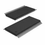 SN74CB3Q16811DL

The activity of extra discounts on wholesale prices is in full swing…
Please fill in your contact information and we will send you the latest wholesale price list.






