 ChipApex | Global Electronic Components Supplier

SEARCH
Search Product
Search Post
— IC芯片 | 连接器 | 传感器 | 被动器件 —
Search productSearch post
— IC芯片 | 连接器 | 传感器 | 被动器件 —
Consult the customer manager about the wholesale price.
consultation hotline:86-132-6715-2157
email:[email protected]
Contact the product manager for consultation. One-stop consultation is available.
Do you want a lower wholesale price? Please send us your inquiry and we will reply immediately.
The SN74CB3Q3125PW is a quadruple FET bus switch in a 14-pin TSSOP package. It operates on a single supply voltage ranging from 2.3V to 3.6V and supports data I/O voltages up to 5.5V. The device features four independent 1-bit switches with separate active-low output-enable inputs. Key electrical parameters include a typical ON-state resistance of 4Ω, a maximum propagation delay of 0.2ns at 3.3V, and a maximum control input switching frequency of 20MHz. It provides rail-to-rail switching capabilities and low off-state capacitance.
Verify the obsolete status of the SN74CB3Q3125PW variant before procurement. Confirm that the active replacement SN74CB3Q3125PWR maintains identical pinout and electrical specifications. Ensure the design accommodates the transition from tube packaging to tape-and-reel formats if required by assembly equipment.
Select this component for applications requiring bidirectional data flow with near-zero propagation delay. It is suitable for broadband communications and networking where low capacitive loading is critical. Verify that the control logic levels match the TTL or CMOS requirements specified in the datasheet.
This part belongs to the SN74CB3Q family of high-speed bus switches. It utilizes a charge pump to elevate gate voltage, providing flat ON-state resistance across the operating range. The PW suffix indicates a 14-lead Thin-Shrink Small-Outline Package (TSSOP) with a body size of 5.00mm x 4.40mm.
SN74CB3Q3125PWR
The SN74CB3Q3125 includes Ioff circuitry that prevents damaging current backflow through the device when it is powered down, allowing for safe isolation during power-off states.
The data I/O ports support signaling levels up to 5.5V, making them compatible with 5V logic systems even when the VCC supply is lower.
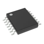 SN74CB3Q3125PW

The activity of extra discounts on wholesale prices is in full swing…
Please fill in your contact information and we will send you the latest wholesale price list.






