 ChipApex | Global Electronic Components Supplier

SEARCH
Search Product
Search Post
— IC芯片 | 连接器 | 传感器 | 被动器件 —
Search productSearch post
— IC芯片 | 连接器 | 传感器 | 被动器件 —
Consult the customer manager about the wholesale price.
consultation hotline:86-132-6715-2157
email:[email protected]
Contact the product manager for consultation. One-stop consultation is available.
Do you want a lower wholesale price? Please send us your inquiry and we will reply immediately.
The SN74CB3Q3253DGVRE4 is a dual 1-of-4 FET multiplexer/demultiplexer bus switch from Texas Instruments. It operates within a VCC range of 2.3V to 3.6V and supports bidirectional data flow with near-zero propagation delay. The device features high-bandwidth data paths up to 500MHz, 5V tolerant I/Os, and low on-state resistance (ron = 4Ω typical). It utilizes a charge pump for flat ON-state resistance characteristics and includes Ioff circuitry for partial-power-down mode operation.
Verify the DGV package designation corresponds to the TVSOP-16 form factor required for your PCB layout. Confirm that the E4 suffix aligns with current environmental compliance standards before finalizing procurement. Ensure control inputs are tied to valid logic levels during power transitions to maintain proper device state.
Select this component when designing systems requiring high-speed signal routing between multiple sources. The dual 1-of-4 configuration allows independent control of two separate data buses. Verify that the 5V tolerant I/Os match the voltage levels of connected peripherals to ensure reliable signal integrity across the operating temperature range.
This part belongs to the SN74CB3Q family of low-voltage high-bandwidth bus switches. It shares functional similarities with other CB3Q devices but offers specific dual multiplexer/demultiplexer architecture. The DGV package provides a compact surface-mount solution suitable for space-constrained designs in consumer electronics and networking equipment.
SN74CB3Q3253DGVR
The SN74CB3Q3253DGVRE4 includes Ioff circuitry that prevents damaging current backflow through the device when it is powered down while the system remains active.
The maximum switching frequency for the OE or S control inputs is specified as 20MHz under recommended operating conditions.
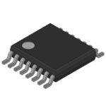 SN74CB3Q3253DGVRE4

The activity of extra discounts on wholesale prices is in full swing…
Please fill in your contact information and we will send you the latest wholesale price list.





