 ChipApex | Global Electronic Components Supplier

SEARCH
Search Product
Search Post
— IC芯片 | 连接器 | 传感器 | 被动器件 —
Search productSearch post
— IC芯片 | 连接器 | 传感器 | 被动器件 —
Consult the customer manager about the wholesale price.
consultation hotline:86-132-6715-2157
email:[email protected]
Contact the product manager for consultation. One-stop consultation is available.
Do you want a lower wholesale price? Please send us your inquiry and we will reply immediately.
The SN74CB3T16211GQLR is a high-speed TTL-compatible FET bus switch from the Widebus family, organized as two independent 12-bit switches within a single VFBGA package. It operates on a supply voltage (VCC) ranging from 2.3 V to 3.6 V and supports bidirectional data flow with near-zero propagation delay. The device features low ON-state resistance (ron = 5 Ω typ) and low input/output capacitance (Cio(OFF) = 5 pF typ). It provides mixed-mode signal operation by translating voltages that track VCC, allowing 5-V tolerant I/Os even when powered down.
Verify the specific GQL suffix indicates the VFBGA package configuration. Confirm RoHS compliance and lead finish details against the latest Package Option Addendum. Ensure design-in requirements match the -40°C to 85°C operating temperature range and the 2.3 V to 3.6 V supply voltage specifications provided in the datasheet.
Select this component for designs requiring low propagation delay and minimal loading on high-speed buses. It is suitable for portable equipment due to low power consumption. Ensure control inputs are driven by TTL or 5-V/3.3-V CMOS outputs. Verify that the system can accommodate the specific VFBGA footprint and thermal characteristics of the GQL package.
This device belongs to Texas Instruments' Widebus family of high-performance bus switches. It is designed to replace older discrete switching solutions by integrating multiple channels into a compact form factor. The SN74CB3T16211 series offers flexibility in configuring 12-bit or 24-bit wide buses depending on the application's pin count and bandwidth requirements.
Check for SN74CB3T16211DGGR or SN74CB3T16211DLR if alternative packages like TSSOP or SSOP are required. Verify functional equivalence regarding voltage translation and pinout compatibility before substitution.
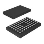 SN74CB3T16211GQLR

The activity of extra discounts on wholesale prices is in full swing…
Please fill in your contact information and we will send you the latest wholesale price list.





