 ChipApex | Global Electronic Components Supplier

SEARCH
Search Product
Search Post
— IC芯片 | 连接器 | 传感器 | 被动器件 —
Search productSearch post
— IC芯片 | 连接器 | 传感器 | 被动器件 —
Consult the customer manager about the wholesale price.
consultation hotline:86-132-6715-2157
email:[email protected]
Contact the product manager for consultation. One-stop consultation is available.
Do you want a lower wholesale price? Please send us your inquiry and we will reply immediately.
The SN74CBT16210CDGVR is a high-speed TTL-compatible FET bus switch from the Widebus family, housed in a 48-pin TVSOP package. It comprises two independent 10-bit switches or one 20-bit switch with separate output-enable inputs. Operating within a VCC range of 4 V to 5.5 V, it supports bidirectional data flow with near-zero propagation delay (typical 0.15 ns at 5 V). The device features low ON-state resistance (3 Ω typical) and low input/output capacitance (5.5 pF typical), minimizing signal distortion. It includes active undershoot protection up to -2 V on A and B ports, Ioff for partial-power-down isolation, and latch-up performance exceeding 100 mA per JESD 78 Class II.
Verify the ordering suffix 'DGVR' corresponds to the TVSOP-48 package and tape-and-reel packaging configuration. Confirm that the component status remains Active as listed in the latest Texas Instruments documentation. Ensure the operating temperature range of -40°C to 85°C aligns with system thermal requirements before finalizing procurement specifications.
Select this component for designs requiring high-speed bidirectional data transfer with minimal propagation delay. The dual 10-bit architecture allows flexible configuration as either separate buses or a single 20-bit path. Consider the low ON-state resistance and capacitance for maintaining signal integrity in high-frequency applications. Verify control input compatibility with the system's logic voltage levels.
This part belongs to the SN74CBT16210C series, which includes variants such as SN74CBT16210CDL, SN74CBT16210CDLR, and SN74CBT16210CDGG. These devices share identical electrical characteristics but differ in package type and shipping configuration. The CDGVR variant specifically utilizes the TVSOP package, distinguishing it from the SSOP and TSSOP options available in the same product family.
Publicly confirmed parameter-equivalent substitutes include SN74CBT16210CDGGR (TSSOP package) and SN74CBT16210CDLR (SSOP package). These alternatives maintain functional equivalence but require verification of package footprint compatibility and reflow profile adherence during replacement planning.
The device incorporates an Ioff feature that prevents damaging current from backflowing through the switch when VCC is zero, ensuring complete isolation between ports during power-off states.
Active undershoot-protection circuitry on the A and B ports provides protection against undershoot events down to -2 V while maintaining the switch in the correct OFF state.
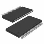 SN74CBT16210CDGVR

The activity of extra discounts on wholesale prices is in full swing…
Please fill in your contact information and we will send you the latest wholesale price list.






