 ChipApex | Global Electronic Components Supplier

SEARCH
Search Product
Search Post
— IC芯片 | 连接器 | 传感器 | 被动器件 —
Search productSearch post
— IC芯片 | 连接器 | 传感器 | 被动器件 —
Consult the customer manager about the wholesale price.
consultation hotline:86-132-6715-2157
email:[email protected]
Contact the product manager for consultation. One-stop consultation is available.
Do you want a lower wholesale price? Please send us your inquiry and we will reply immediately.
The SN74CBT16210CDL is a high-speed TTL-compatible FET bus switch from the Widebus family, housed in a 48-pin SSOP package. It features two independent 10-bit switches or one 20-bit configuration with separate output-enable inputs. Operating within a supply voltage range of 4 V to 5.5 V, it supports data I/O levels from 0 V to 5 V. The device exhibits low ON-state resistance (typically 3 Ω at 4.5 V) and near-zero propagation delay (150 ps at 5 V). It includes active undershoot protection up to -2 V on A and B ports, ensuring isolation during partial-power-down via the Ioff feature.
Verify the specific ordering suffix 'DL' corresponds to the SSOP-48 tube packaging format required for your assembly process. Confirm that the operating temperature range of -40°C to 85°C aligns with your environmental specifications. Ensure control inputs are tied to VCC or GND to maintain the high-impedance state during power-up sequences.
Select this component when designing systems requiring wide-bus switching with minimal signal distortion. It is suitable for applications needing support for multiple signaling levels including 1.8-V, 2.5-V, 3.3-V, and 5-V. Consider its latch-up performance exceeding 100 mA per JESD 78 Class II if robustness against ESD events is critical.
This device belongs to Texas Instruments' Widebus family of high-speed FET bus switches. It shares functional similarities with other members like the SN74CBT16212 but differs in bit width and pinout configuration. The SN74CBT16210C series provides a solution for managing large data buses where low capacitance and fast switching speeds are necessary to maintain signal integrity.
The SN74CBT16210CDLR serves as the tape-and-reel equivalent of the SN74CBT16210CDL. Other variants include the SN74CBT16210CDGG (TSSOP) and SN74CBT16210CDGVR (TVSOP). Verify pin compatibility and package dimensions before substituting with these alternative packages.
The SN74CBT16210CDL supports partial-power-down mode through its Ioff feature. This ensures that no damaging current flows back through the device when VCC is zero, maintaining isolation between powered and unpowered sections of the system.
The device features active undershoot-protection circuitry on both the A and B ports. This allows the ports to tolerate undershoot voltages down to -2 V without compromising the OFF state of the switch.
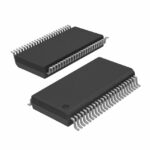 SN74CBT16210CDL

The activity of extra discounts on wholesale prices is in full swing…
Please fill in your contact information and we will send you the latest wholesale price list.





