 ChipApex | Global Electronic Components Supplier

SEARCH
Search Product
Search Post
— IC芯片 | 连接器 | 传感器 | 被动器件 —
Search productSearch post
— IC芯片 | 连接器 | 传感器 | 被动器件 —
Consult the customer manager about the wholesale price.
consultation hotline:86-132-6715-2157
email:[email protected]
Contact the product manager for consultation. One-stop consultation is available.
Do you want a lower wholesale price? Please send us your inquiry and we will reply immediately.
The SN74CBT16233DGG is a 16-bit 1-of-2 FET multiplexer/demultiplexer housed in a 56-pin TSSOP package. It operates within a supply voltage range of 4.75 V to 5.25 V and supports an operating temperature range from -40°C to +85°C. The device features TTL-compatible input levels and provides a low on-state resistance, typically 5 Ω at VCC = 5 V with II = 64 mA. Control inputs SEL1, SEL2, and TEST can be driven by 5-V CMOS, 5-V TTL, or low-voltage TTL drivers.
Verify the specific ordering suffix matches the required package type, as the base part number covers multiple variants including DGV and DL packages. Confirm RoHS compliance status and moisture sensitivity level ratings prior to procurement. Ensure that unused control inputs are properly terminated to VCC or GND during operation to maintain device reliability and proper functionality.
Select this component when a 16-bit wide bus switch with 1-of-2 selection logic is required. The device is suitable for applications needing simultaneous addressing of two memory banks or consolidating dual data paths into a single line. Consider the 56-pin TSSOP form factor for board space constraints and verify compatibility with 5-V logic driver interfaces.
This device belongs to Texas Instruments' Widebus family of high-speed bus switches. It is designed for applications requiring efficient multiplexing of wide data buses. The SN74CBT16233 serves as a core component for managing data flow in systems where multiple sources must share a common destination or vice versa.
Public confirmed substitute part numbers: None identified in source material.
When TEST inputs are asserted, the A port is connected to both the B1 and B2 ports simultaneously, allowing for parallel data transmission.
The SEL1, SEL2, and TEST inputs can be driven by 5-V CMOS, 5-V TTL, or low-voltage TTL drivers due to their TTL-compatible input levels.
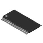 SN74CBT16233DGG

The activity of extra discounts on wholesale prices is in full swing…
Please fill in your contact information and we will send you the latest wholesale price list.






