 ChipApex | Global Electronic Components Supplier

SEARCH
Search Product
Search Post
— IC芯片 | 连接器 | 传感器 | 被动器件 —
Search productSearch post
— IC芯片 | 连接器 | 传感器 | 被动器件 —
Consult the customer manager about the wholesale price.
consultation hotline:86-132-6715-2157
email:[email protected]
Contact the product manager for consultation. One-stop consultation is available.
Do you want a lower wholesale price? Please send us your inquiry and we will reply immediately.
The SN74CBT16811CDL is a high-speed TTL-compatible FET bus switch from the Widebus family, organized as two independent 12-bit switches or one 24-bit switch. It operates within a VCC range of 4V to 5.5V and supports data I/O signaling levels from 0V to 5.5V. The device features low ON-state resistance (ron) for minimal propagation delay and includes active undershoot protection on A and B ports up to -2V. It incorporates a precharged B port via a user-selectable bias voltage (BIASV) to minimize live-insertion noise.
Verify that the DL package designation corresponds to the SSOP form factor when sourcing. Confirm the operating temperature range matches the application requirements of -40°C to 85°C. Ensure control inputs are tied to VCC or GND to maintain proper device operation. Check datasheet specifications for thermal impedance values relevant to the specific PCB layout and ambient conditions.
Select this component for designs requiring wide-voltage translation between 0V and 5.5V domains while maintaining a single 4V to 5.5V supply. The device is suitable for applications demanding low loading due to its low input/output capacitance. Consider the separate output-enable inputs if independent control of the two 12-bit sections is required rather than a unified 24-bit switch.
This part belongs to Texas Instruments' Widebus family of high-speed bus switches. It is designed to provide low ON-state resistance and fast switching speeds. The SN74CBT16811C variant specifically addresses live-insertion noise through bias voltage precharging and offers robust protection against undershoot events on the data ports.
SN74CBT16811CDGGR is an equivalent part number in the TSSOP-56 package offering tape-and-reel packaging instead of the tube-packaged SSOP-DL format.
The B port is precharged to a user-selectable bias voltage (BIASV) through an equivalent 10-kΩ resistor when OE is high or the device is powered down. This minimizes glitches caused by parasitic capacitance during card insertion or removal.
The Ioff feature ensures that damaging current will not backflow through the device when it is powered down (VCC = 0 V), providing isolation during partial-power-down applications.
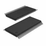 SN74CBT16811CDL

The activity of extra discounts on wholesale prices is in full swing…
Please fill in your contact information and we will send you the latest wholesale price list.




