 ChipApex | Global Electronic Components Supplier
SEARCH
Search Product
Search Post
— IC芯片 | 连接器 | 传感器 | 被动器件 —
Search productSearch post
— IC芯片 | 连接器 | 传感器 | 被动器件 —
Consult the customer manager about the wholesale price.
consultation hotline:86-132-6715-2157
email:[email protected]
Contact the product manager for consultation. One-stop consultation is available.
Do you want a lower wholesale price? Please send us your inquiry and we will reply immediately.
The SN74CBT3306PW is a dual FET bus switch from Texas Instruments' CBT logic series, housed in an 8-pin TSSOP package. It operates within a supply voltage range of 4.5 V to 5.5 V and supports data I/O levels from 0 V to 5.5 V. The device features two independent 1:1 switches with separate output enable inputs. Key electrical characteristics include a maximum on-resistance of 14 Ω at 4 V and a propagation delay of 0.35 ns at 4 V with a 50 pF load. It functions reliably across an operating temperature range of -40 °C to +85 °C.
Verify the specific suffix 'PW' corresponds to the 8-TSSOP package variant when sourcing. Confirm RoHS compliance status and moisture sensitivity level (MSL 1) requirements against your assembly process specifications. Ensure the supply voltage aligns with the 4.5 V to 5.5 V operational range defined in the datasheet.
Select this component for designs requiring TTL-compatible control inputs driven by 5 V or 3.3 V CMOS outputs. The low input/output capacitance minimizes signal distortion and loading effects. Consider the 8-TSSOP package dimensions if board space is constrained compared to standard SOIC options.
This part belongs to the SN74CBT3306 family of high-speed bus switches. Variants such as SN74CBT3306D utilize an SOIC-8 package, while SN74CBT3306PWR uses a PowerTSSOP-8 package. All variants share the same core dual-channel functionality but differ in physical footprint and thermal characteristics.
SN74CBT3306D serves as a pin-compatible alternative in an SOIC-8 package. SN74CBT3306PWR offers a similar surface-mount solution in a PowerTSSOP-8 package. Verify package dimensions and thermal resistance values before substitution.
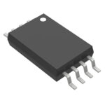 SN74CBT3306PW
The activity of extra discounts on wholesale prices is in full swing…
Please fill in your contact information and we will send you the latest wholesale price list.






