 ChipApex | Global Electronic Components Supplier
SEARCH
Search Product
Search Post
— IC芯片 | 连接器 | 传感器 | 被动器件 —
Search productSearch post
— IC芯片 | 连接器 | 传感器 | 被动器件 —
Consult the customer manager about the wholesale price.
consultation hotline:86-132-6715-2157
email:[email protected]
Contact the product manager for consultation. One-stop consultation is available.
Do you want a lower wholesale price? Please send us your inquiry and we will reply immediately.
The SN74CBT3383CDGVR is a high-speed TTL-compatible FET bus-exchange switch manufactured by Texas Instruments. It operates within a supply voltage range of 4 V to 5.5 V and supports data I/O levels from 0 V to 5 V. The device features low ON-state resistance (ron) with typical values of 3 Ω at 4.5 V and 6 Ω at 4 V, ensuring minimal propagation delay. It includes active undershoot protection on A and B ports up to -2 V and offers an Ioff feature for partial-power-down mode operation.
Verify the specific package marking CU383C and orderable part number SN74CBT3383CDGVR against the manufacturer's latest documentation. Confirm that the TVSOP-24 (DGV) package dimensions and thermal impedance specifications align with your PCB layout requirements. Ensure all unused control inputs are tied to VCC or GND to maintain proper device operation and prevent floating states.
Select this component when bidirectional data exchange between four signal ports is required alongside standard bus switching capabilities. The device is suitable for applications demanding low power consumption with a maximum ICC of 3 µA. Consider the TVSOP-24 package if space constraints require a compact surface-mount solution while maintaining robust latch-up performance exceeding 100 mA per JESD 78 standards.
This device belongs to the SN74CBT3383C series of high-speed FET bus switches. It is designed for applications requiring fast switching speeds and low signal distortion. The DGV suffix indicates the TVSOP-24 tape-and-reel packaging format. The product is classified as active, meaning it is recommended for new designs and remains in production by Texas Instruments.
Consult the official datasheet for direct pin-compatible alternatives within the same family. Verify electrical characteristics such as ron and tpd when substituting with other bus switches to ensure signal integrity is maintained in the target application.
The device supports partial-power-down mode via the Ioff feature. When VCC is 0 V and the switch is off, Ioff ensures that no more than 10 µA flows through the I/O pins, preventing damaging backflow current into the powered-down system.
The BE (bus-exchange enable) input controls the connection state between the A and B ports. When BE is low, the ports connect; when high, they disconnect. The BX input determines the data path configuration when BE is low, allowing the A port to map to either the B1 or B2 port group.
Yes, the SN74CBT3383CDGVR includes active undershoot-protection circuitry on the A and B ports. This feature senses undershoot events and ensures the switch remains in the proper OFF state, protecting against signals as low as -2 V.
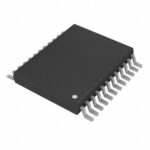 SN74CBT3383CDGVR
The activity of extra discounts on wholesale prices is in full swing…
Please fill in your contact information and we will send you the latest wholesale price list.





