 ChipApex | Global Electronic Components Supplier
SEARCH
Search Product
Search Post
— IC芯片 | 连接器 | 传感器 | 被动器件 —
Search productSearch post
— IC芯片 | 连接器 | 传感器 | 被动器件 —
Consult the customer manager about the wholesale price.
consultation hotline:86-132-6715-2157
email:[email protected]
Contact the product manager for consultation. One-stop consultation is available.
Do you want a lower wholesale price? Please send us your inquiry and we will reply immediately.
The SN74CBT6800ADW is a 10-bit FET bus switch manufactured by Texas Instruments, housed in a 24-pin SOIC (DW) package. It operates within a supply voltage range of 4 V to 5.5 V and supports an operating temperature from -40°C to 85°C. The device features TTL-compatible input levels and provides bidirectional switching with near-zero propagation delay. Key electrical parameters include a maximum on-state resistance of 20 Ω at VCC = 4 V and a typical propagation delay of 0.35 ns at VCC = 4 V. The B port precharges to a user-selectable bias voltage via an equivalent 10-kΩ resistor when disabled.
Verify the specific ordering suffix 'DW' corresponds to the SOIC-24 tube packaging configuration. Confirm the component status as active production data per the manufacturer's documentation. Ensure compatibility with the specified 4 V to 5.5 V supply voltage range and -40°C to 85°C operating temperature limits for your application environment.
Select this component for designs requiring 10-bit wide bus switching with minimal propagation delay. The precharged output feature is critical for applications involving live insertion to reduce noise. Ensure control inputs are held at VCC or GND to prevent floating states. Verify that the load capacitance and current requirements fall within the absolute maximum ratings defined in the datasheet.
This part belongs to the SN74CBT6800A series of 10-bit FET bus switches. It is functionally similar to other variants like the SN74CBTK6800 but includes specific precharge capabilities. The DW suffix indicates the standard SOIC package format, distinct from TSSOP or SSOP options available in the same family.
Direct substitutes include SN74CBT6800APWR (TSSOP package) and SN74CBT6800ADBQ (SSOP package). Verify pinout compatibility and package dimensions before substitution. Other family members may lack the specific precharge functionality or have different pin configurations.
When the ON input is high or VCC is 0 V, the B port is precharged to the BIASV level through an equivalent 10-kΩ resistor, minimizing signal distortion and noise during live insertion events.
When the ON input is high, the switch between Port A and Port B is open (high impedance), and the B port is precharged to the BIASV voltage.
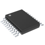 SN74CBT6800ADW
The activity of extra discounts on wholesale prices is in full swing…
Please fill in your contact information and we will send you the latest wholesale price list.






