 ChipApex | Global Electronic Components Supplier
SEARCH
Search Product
Search Post
— IC芯片 | 连接器 | 传感器 | 被动器件 —
Search productSearch post
— IC芯片 | 连接器 | 传感器 | 被动器件 —
Consult the customer manager about the wholesale price.
consultation hotline:86-132-6715-2157
email:[email protected]
Contact the product manager for consultation. One-stop consultation is available.
Do you want a lower wholesale price? Please send us your inquiry and we will reply immediately.
The SN74CBT6800CDBQRE4 is a 10-bit FET bus switch from the Widebus family, housed in a 24-pin DBQ (QSOP) package. It operates within a VCC range of 4 V to 5.5 V and supports data I/O levels from 0 V to 5 V. The device features low ON-state resistance (ron), with typical values of 3 Ω at VI=0 and 5 V at VI=2.4 V. It provides active undershoot protection on A and B ports up to -2 V and precharges the B port via a user-selectable BIASV pin to minimize live-insertion noise. Propagation delay is typically 0.15 ns at 5 V.
Verify the specific ordering suffix 'E4' indicates lead-free/RoHS compliance status as per Texas Instruments documentation. Confirm the DBQ package designation matches the required QSOP footprint for PCB layout. Ensure the BIASV pin connection aligns with the target receiver input threshold voltage to effectively mitigate live-insertion glitches. Cross-reference the datasheet revision date against manufacturing lot dates for compatibility.
Select this component when designing high-speed digital buses requiring bidirectional switching with minimal signal degradation. The device is suitable for environments where live insertion occurs, leveraging its precharge capability. Ensure control inputs are driven by TTL or 5-V/3.3-V CMOS outputs. Verify that the operating temperature range of -40°C to 85°C meets system environmental requirements.
This part belongs to the SN74CBT6800 series, a family of high-speed TTL-compatible FET bus switches. The 'C' variant denotes specific electrical characteristics including undershoot protection. The 'DBQ' suffix identifies the 24-lead Thin Shrink Small Outline Package (QSOP). The 'RE4' suffix typically denotes tape-and-reel packaging with lead-free finish.
SN74CBT6800CDGVR is an alternative within the same family using a TVSOP package. SN74CBT6800CPWR offers the same functionality in a TSSOP package. Verify pinout compatibility and thermal performance differences between packages before substitution.
The BIASV pin precharges the B port to a user-selectable voltage level. This ensures that any glitch produced by card insertion does not cross the input threshold region of receivers on the active bus, minimizing live-insertion noise.
The Ioff feature allows the device to support partial-power-down mode. It ensures that damaging current will not backflow through the device when it is powered down, providing isolation during power-off states.
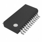 SN74CBT6800CDBQRE4
The activity of extra discounts on wholesale prices is in full swing…
Please fill in your contact information and we will send you the latest wholesale price list.





