 ChipApex | Global Electronic Components Supplier
SEARCH
Search Product
Search Post
— IC芯片 | 连接器 | 传感器 | 被动器件 —
Search productSearch post
— IC芯片 | 连接器 | 传感器 | 被动器件 —
Consult the customer manager about the wholesale price.
consultation hotline:86-132-6715-2157
email:[email protected]
Contact the product manager for consultation. One-stop consultation is available.
Do you want a lower wholesale price? Please send us your inquiry and we will reply immediately.
The SN74CBT6845CDW is an 8-bit FET bus switch manufactured by Texas Instruments, housed in a 20-pin SOIC (DW) package. It operates within a supply voltage range of 4 V to 5.5 V and supports data I/O levels from 0 V to 5 V. The device features low ON-state resistance with a maximum value of 12 Ω at VCC = 4 V and 6 Ω at VCC = 4.5 V. Propagation delay is specified as a maximum of 0.24 ns at VCC = 4 V and 0.15 ns at VCC = 5 V. It includes active undershoot protection up to -2 V on the A and B ports and precharges the B port via a bias voltage (BIASV). The component functions across a temperature range of -40°C to +85°C.
Verify the specific ordering suffix 'DW' corresponds to the SOIC-20 tube packaging configuration. Confirm that the required operating temperature range aligns with the industrial specification of -40°C to +85°C. Ensure the design accommodates the 4 V to 5.5 V supply voltage requirements and utilizes the BIASV pin for optimal performance in live-insertion scenarios. Check for any recent product change notifications regarding this part number.
Select this component for designs requiring high-speed bidirectional switching with minimal signal degradation. The integrated undershoot protection and BIASV precharging make it suitable for systems prone to connector glitches during insertion. Ensure control inputs are driven by compatible TTL or CMOS logic levels. Consider the thermal impedance characteristics of the SOIC package if significant power dissipation is expected in the application environment.
This device belongs to the SN74CBT6845C family of high-speed TTL-compatible FET bus switches. It is designed to provide low ON-state resistance and minimal propagation delay for efficient data transfer. The family supports both digital and analog applications, offering robust isolation and signal integrity features essential for modern high-speed bus architectures.
SN74CBT6845CPW (TSSOP-20 package)
The B port is precharged to a user-selectable bias voltage (BIASV) when the switch is off. This minimizes glitching effects during card insertion by ensuring signals do not cross the input threshold region of receivers on the active bus.
The Ioff feature ensures that damaging current will not backflow through the device when it is powered down (VCC = 0 V), providing isolation during partial-power-down applications.
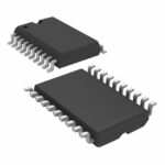 SN74CBT6845CDW
The activity of extra discounts on wholesale prices is in full swing…
Please fill in your contact information and we will send you the latest wholesale price list.





