 ChipApex | Global Electronic Components Supplier
SEARCH
Search Product
Search Post
— IC芯片 | 连接器 | 传感器 | 被动器件 —
Search productSearch post
— IC芯片 | 连接器 | 传感器 | 被动器件 —
Consult the customer manager about the wholesale price.
consultation hotline:86-132-6715-2157
email:[email protected]
Contact the product manager for consultation. One-stop consultation is available.
Do you want a lower wholesale price? Please send us your inquiry and we will reply immediately.
The SN74CBTD3306CPWRG4 is a dual FET bus switch from Texas Instruments, featuring level shifting and -2 V undershoot protection. It operates within a supply voltage range of 4.5 V to 5.5 V. The device provides two independent channels in an 8-pin TSSOP package. Key electrical characteristics include a maximum on-resistance of 16.5 ohms and a propagation delay of 1.4 ns at 5 V with a 50 pF load. It supports high output currents of up to 128 mA and functions reliably across an industrial temperature range of -40 °C to +85 °C.
Verify the specific suffix 'G4' indicates lead-free compliance and RoHS status as per manufacturer documentation. Confirm the 'C' designator corresponds to the specified operating temperature range and package variant. Cross-reference the full part number with official Texas Instruments databases to ensure availability and current manufacturing status before finalizing procurement plans.
Select this component when designing circuits requiring bidirectional bus switching with integrated level shifting. Ensure the system voltage remains within the 4.5 V to 5.5 V operational window. Consider the 16.5 ohm on-resistance for signal integrity requirements. Verify that the TSSOP-8 package dimensions fit the PCB layout constraints and thermal management needs of the application.
This device belongs to the SN74CBT series of digital bus switches. It shares functional similarities with other members like the SN74CBTD3306CDR but differs in packaging and specific environmental ratings. The CBTD series is designed for applications demanding low power consumption and high-speed performance in compact form factors.
The SN74CBTD3306CDR is a documented alternative offering similar functionality in an SOIC package. Verify pin compatibility and thermal performance differences when substituting. Ensure the replacement meets the same voltage and temperature specifications required by the original design.
Yes, as a dual FET bus switch, it allows signals to pass in either direction between the input and output pins when enabled.
It protects the internal circuitry from damage caused by negative voltage transients or undershoot events that may occur during signal transitions.
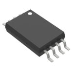 SN74CBTD3306CPWRG4
The activity of extra discounts on wholesale prices is in full swing…
Please fill in your contact information and we will send you the latest wholesale price list.





