 ChipApex | Global Electronic Components Supplier
SEARCH
Search Product
Search Post
— IC芯片 | 连接器 | 传感器 | 被动器件 —
Search productSearch post
— IC芯片 | 连接器 | 传感器 | 被动器件 —
Consult the customer manager about the wholesale price.
consultation hotline:86-132-6715-2157
email:[email protected]
Contact the product manager for consultation. One-stop consultation is available.
Do you want a lower wholesale price? Please send us your inquiry and we will reply immediately.
The SN74CBTD3306D is a dual FET bus switch from Texas Instruments, featuring level shifting and -2 V undershoot protection. It operates within a supply voltage range of 4.5 V to 5.5 V. The device contains two independent switches in an 8-pin SOIC package. Key electrical parameters include a maximum on-resistance of 35 Ω, a maximum high-level output current of -128 mA, and a maximum low-level output current of 128 mA. Propagation delay is specified at 0.25 ns at 5 V with a 50 pF load. Operating temperature ranges from -40 °C to +85 °C.
Verify the specific suffix 'D' corresponds to the standard SOIC-8 package configuration. Confirm that the operating voltage requirements align with the 4.5 V to 5.5 V specification. Ensure thermal management meets the -40 °C to +85 °C industrial temperature range requirements. Check for RoHS compliance status if required by project specifications.
Select this component when a dual-channel bus switch with level shifting is required for 5 V logic systems. Consider the 35 Ω on-resistance for signal loss calculations. Evaluate the 8-pin SOIC footprint against available PCB space. Compare propagation delay characteristics against system timing constraints to ensure signal integrity is maintained.
This part belongs to the SN74CBT series of bus switches designed for high-speed applications. It is distinct from the SN74CB3Q3306A which operates at lower voltages (2.3 V to 3.6 V) and offers lower on-resistance. The SN74CBTD3306D is specifically optimized for 5 V operation with added protection features compared to basic switches.
SN74CBTD3306DR is the tape-and-reel version of the same device. SN74CBTD3306CDR is a variant with similar functionality but may have slight parameter differences. Verify pinout compatibility before substitution.
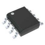 SN74CBTD3306D
The activity of extra discounts on wholesale prices is in full swing…
Please fill in your contact information and we will send you the latest wholesale price list.





