 ChipApex | Global Electronic Components Supplier
SEARCH
Search Product
Search Post
— IC芯片 | 连接器 | 传感器 | 被动器件 —
Search productSearch post
— IC芯片 | 连接器 | 传感器 | 被动器件 —
Consult the customer manager about the wholesale price.
consultation hotline:86-132-6715-2157
email:[email protected]
Contact the product manager for consultation. One-stop consultation is available.
Do you want a lower wholesale price? Please send us your inquiry and we will reply immediately.
The SN74CBTS3306PWR is a dual FET bus switch featuring Schottky diode clamping, designed for 5-V applications. It contains two single-pole, single-throw (SPST) circuits in an 8-pin TSSOP package. The device operates within a supply voltage range of 4.5 V to 5.5 V and supports temperatures from -40 °C to +85 °C. Key electrical parameters include a maximum on-resistance of 35 Ω, a maximum propagation delay of 0.25 ns at 5 V with 50 pF load, and output currents of ±128 mA.
Verify the specific suffix 'PWR' corresponds to the TSSOP-8 package and tape-and-reel delivery format as defined by Texas Instruments. Confirm that the component meets RoHS compliance standards required for your assembly process. Ensure that unused control inputs are properly terminated to VCC or GND during implementation to guarantee stable operation. Cross-reference the datasheet revision to ensure compatibility with current manufacturing specifications.
Select this component when a 5-V logic interface requires bidirectional switching with overvoltage protection. The integrated Schottky diodes eliminate the need for external clamping components, reducing board space. Compare the 35 Ω on-resistance against system impedance requirements to minimize signal attenuation. Consider the TSSOP-8 footprint constraints relative to available PCB real estate.
This part belongs to the SN74CBT family of bus switches, which are optimized for low power consumption and fast switching speeds. It serves as a functional alternative to standard logic buffers where signal isolation or direction control is necessary. The inclusion of Schottky clamping distinguishes it from basic switches like the SN74CBTD3306, offering enhanced protection against voltage spikes on the bus lines.
The SN74CBTD3306D may serve as a substitute if Schottky clamping is not required, though it lacks the specific overvoltage protection features. Verify pinout compatibility and electrical parameter alignment before substitution.
The integrated Schottky diodes provide clamping protection to prevent undershoot or overshoot voltages from damaging the connected circuitry or causing latch-up conditions.
All unused control inputs must be held at VCC or GND to ensure proper device operation and prevent undefined states.
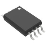 SN74CBTS3306PWR
The activity of extra discounts on wholesale prices is in full swing…
Please fill in your contact information and we will send you the latest wholesale price list.






