 ChipApex | Global Electronic Components Supplier

SEARCH
Search Product
Search Post
— IC芯片 | 连接器 | 传感器 | 被动器件 —
Search productSearch post
— IC芯片 | 连接器 | 传感器 | 被动器件 —
Consult the customer manager about the wholesale price.
consultation hotline:86-132-6715-2157
email:[email protected]
Contact the product manager for consultation. One-stop consultation is available.
Do you want a lower wholesale price? Please send us your inquiry and we will reply immediately.
SN74F125NSR is listed in the Buffers, Drivers, Receivers, Transceivers range at ChipApex. The manufacturer field lists Texas Instruments. Its product description is IC BUFFER NON-INVERT 5.5V 14SOP. Review the specifications below when checking this part for your BOM.
The SN74F125NSR is a quadruple bus buffer gate with 3-state outputs manufactured by Texas Instruments. It operates within a supply voltage range of 4.5 V to 5.5 V and features four independent non-inverting line drivers. Each output is disabled when the associated output-enable (OE) input is high. The device utilizes an SOP-14 package and supports surface-mount installation. Electrical characteristics include a high-level output current of -15 mA and a low-level output current of 64 mA at 5 V. Propagation delay times are specified between 1.2 ns and 8 ns depending on conditions.
Verify that the component matches the SN74F125NSR designation and SOP-14 package configuration. Confirm the operating temperature range aligns with the 0°C to 70°C specification. Ensure the logic family corresponds to the F series requirements for your circuit design. Cross-reference the datasheet revision date to confirm parameter accuracy.
Select this component when a quadruple bus buffer with 3-state outputs is required for standard 5 V logic applications. The F logic family provides specific drive capabilities suitable for interfacing with various digital systems. Verify that the input voltage levels meet the VIH and VIL specifications for reliable operation within the recommended operating conditions.
This part belongs to the SN74F125 logic family, which consists of quadruple bus buffers with 3-state outputs. The NS suffix indicates the Small Outline Package (SOP) variant. The device is designed for use in digital systems requiring isolated signal paths and bus management capabilities under standard industrial temperature ranges.
SN74AHC125NSRG4
Each output is enabled when the associated output-enable (OE) input is low and disabled when OE is high, regardless of the A input state.
The maximum recommended operating supply voltage (VCC) is 5.5 V.
Explore related parts through Logic, Integrated Circuits (ICs), all product categories, ChipApex homepage.
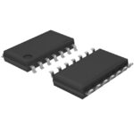 SN74F125NSR

The activity of extra discounts on wholesale prices is in full swing…
Please fill in your contact information and we will send you the latest wholesale price list.





