 ChipApex | Global Electronic Components Supplier
SEARCH
Search Product
Search Post
— IC芯片 | 连接器 | 传感器 | 被动器件 —
Search productSearch post
— IC芯片 | 连接器 | 传感器 | 被动器件 —
Consult the customer manager about the wholesale price.
consultation hotline:86-132-6715-2157
email:[email protected]
Contact the product manager for consultation. One-stop consultation is available.
Do you want a lower wholesale price? Please send us your inquiry and we will reply immediately.
The SN74F151BNE4 is an 8-line to 1-line multiplexer from the Texas Instruments F logic family, housed in a 16-pin PDIP package. It provides full binary decoding to select one of eight data sources based on three address inputs (A, B, C). The device features active-low strobe functionality and complementary outputs (Y and W). Recommended operating conditions specify a supply voltage range of 4.5 V to 5.5 V. Electrical characteristics indicate a typical propagation delay of 9.5 ns for the A/B/C-to-W path at 5 V. Operating temperature range is defined from 0°C to 70°C.
Verify that the specific ordering suffix 'E4' corresponds to the required lead finish and RoHS compliance status as listed in the Package Option Addendum. Confirm the package type matches the design requirements, as this part number specifically denotes the PDIP variant. Ensure the application environment remains within the specified commercial temperature limits of 0°C to 70°C.
Select this component when high-speed switching is required within standard TTL voltage levels. The F series offers faster propagation delays compared to HC or HCT families but consumes more power. Verify that the PCB layout supports through-hole mounting for the 16-pin DIP configuration. Consider the complementary outputs if both true and complemented signals are needed for downstream logic stages.
This device belongs to the SN74F151B family of monolithic data selectors. It serves as a standard solution for routing multiple digital signals onto a single line under control of binary address inputs. The 'N' suffix indicates the plastic dual in-line package option, while 'E4' typically signifies environmental compliance attributes defined by the manufacturer's packaging standards.
SN74F151BN
When the strobe input is at a high logic level, the Y output is forced low and the W output is forced high, regardless of the state of the data or address inputs.
The recommended operating conditions specify a maximum supply voltage (VCC) of 5.5 V.
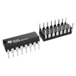 SN74F151BNE4
The activity of extra discounts on wholesale prices is in full swing…
Please fill in your contact information and we will send you the latest wholesale price list.






