 ChipApex | Global Electronic Components Supplier
SEARCH
Search Product
Search Post
— IC芯片 | 连接器 | 传感器 | 被动器件 —
Search productSearch post
— IC芯片 | 连接器 | 传感器 | 被动器件 —
Consult the customer manager about the wholesale price.
consultation hotline:86-132-6715-2157
email:[email protected]
Contact the product manager for consultation. One-stop consultation is available.
Do you want a lower wholesale price? Please send us your inquiry and we will reply immediately.
The SN74GTL16923DGGR is an 18-bit registered bus transceiver from the Widebus family, partitioned into two independent 9-bit sections. It provides LVTTL-to-GTL/GTL+ and GTL/GTL+-to-LVTTL signal-level translation for mixed-mode systems. The device operates with a supply voltage range of 3.15 V to 3.45 V and supports clock frequencies up to 200 MHz. It features D-type flip-flops with qualified storage enable, Ioff support for partial-power-down mode, and active bus-hold circuitry on data inputs. The component is housed in a 64-pin TSSOP (DGG) package.
Verify that the specific orderable part number matches the required package type and temperature rating. Confirm RoHS compliance status and lead finish specifications against the latest manufacturer documentation. Ensure design compatibility with the recommended operating conditions, specifically the 3.15 V to 3.45 V supply voltage range and appropriate termination voltages for the selected logic standard.
Select this component when interfacing LVTTL devices with GTL or GTL+ backplanes. The dual 9-bit architecture allows independent output-enable controls for each section. Consider the device's ability to handle mixed 3.3-V and 5-V input environments. Verify that the system timing requirements align with the specified setup and hold times for the chosen clock frequency and logic standard.
This device belongs to the Texas Instruments Widebus family, designed for high-speed data transmission. It utilizes OEC circuitry to improve signal integrity and reduce electromagnetic interference. The SN74GTL16923 is part of a broader series of registered bus transceivers intended for complex digital systems requiring reliable level shifting and data registration across different voltage domains.
Consult official substitution guides for compatible parts within the same logic family. Verify pinout compatibility and electrical characteristics before replacing existing components in established designs.
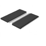 SN74GTL16923DGGR
The activity of extra discounts on wholesale prices is in full swing…
Please fill in your contact information and we will send you the latest wholesale price list.





