 ChipApex | Global Electronic Components Supplier
SEARCH
Search Product
Search Post
— IC芯片 | 连接器 | 传感器 | 被动器件 —
Search productSearch post
— IC芯片 | 连接器 | 传感器 | 被动器件 —
Consult the customer manager about the wholesale price.
consultation hotline:86-132-6715-2157
email:[email protected]
Contact the product manager for consultation. One-stop consultation is available.
Do you want a lower wholesale price? Please send us your inquiry and we will reply immediately.
The SN74HCS138QBQBRQ1 is an automotive-qualified, high-speed silicon gate CMOS decoder featuring three address select inputs and eight active-low outputs. It operates within a supply voltage range of 2 V to 6 V and supports temperatures from -40°C to +125°C. The device utilizes Schmitt-trigger inputs for noise tolerance and includes balanced push-pull outputs capable of ±7.8-mA drive at 6 V. Propagation delays range from 7 ns to 22 ns depending on voltage and temperature. It is housed in a 16-pin WQFN (WBQB) package with wettable flanks.
Verify that the specific WBQB package variant matches the intended PCB footprint and thermal requirements. Confirm AEC-Q100 qualification aligns with project grade specifications. Ensure input termination strategies account for Schmitt-trigger characteristics to prevent undefined states. Validate power supply decoupling practices against the recommended layout guidelines to maintain signal integrity.
Select this component when automotive reliability and wide voltage operation are required. The Schmitt-trigger inputs make it suitable for noisy environments or slow signal edges. Consider the WQFN package for compact designs requiring effective thermal dissipation and inspection visibility. Verify that the output drive strength meets the load requirements without exceeding absolute maximum ratings.
This part belongs to the SN74HCS138-Q1 family of 3-to-8 line decoders/demultiplexers. It shares functional similarities with other HCS series logic devices but is specifically optimized for automotive use. The WBQB suffix denotes the wettable flank WQFN package, distinguishing it from standard QFN or SOIC variants within the same logical family.
SN74HCS138DYYRQ1
Driving inputs with slow transitioning signals increases dynamic current consumption. However, holding an input at a valid non-supply value does not cause huge increases in static power consumption compared to standard CMOS inputs.
The strobe inputs simplify cascading and facilitate demultiplexing. When any strobe input is active, all outputs are forced into the high state. When disabled, only the selected output goes low.
No. Unused outputs should be left floating. Connecting them directly to VCC or ground can cause excessive current flow and damage the device due to the push-pull output structure.
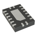 SN74HCS138QBQBRQ1
The activity of extra discounts on wholesale prices is in full swing…
Please fill in your contact information and we will send you the latest wholesale price list.






