 ChipApex | Global Electronic Components Supplier
SEARCH
Search Product
Search Post
— IC芯片 | 连接器 | 传感器 | 被动器件 —
Search productSearch post
— IC芯片 | 连接器 | 传感器 | 被动器件 —
Consult the customer manager about the wholesale price.
consultation hotline:86-132-6715-2157
email:[email protected]
Contact the product manager for consultation. One-stop consultation is available.
Do you want a lower wholesale price? Please send us your inquiry and we will reply immediately.
The SN74HCS237QPWRQ1 is an automotive-qualified, high-speed CMOS decoder/demultiplexer featuring latched address inputs and Schmitt-trigger functionality. It converts three binary address lines into one of eight active-high outputs. The device operates within a supply voltage range of 2 V to 6 V and supports an ambient temperature range from -40°C to +125°C. It utilizes a 16-pin TSSOP package.
Verify the specific suffix 'PW' corresponds to the TSSOP-16 package variant required for your design. Confirm that the Q1 designation aligns with your automotive qualification standards. Ensure compatibility with your system's voltage levels and thermal management capabilities before finalizing procurement.
Select this component when latching address inputs are necessary to maintain output states during bus fluctuations. The Schmitt-trigger inputs make it suitable for noisy environments or applications with slow-rising signals. Verify that the 16-pin TSSOP footprint matches your PCB layout constraints.
This part belongs to the SN74HCS series of high-speed CMOS logic devices. The HCS designation indicates the inclusion of Schmitt-trigger inputs for improved noise rejection. The Q1 suffix denotes automotive qualification according to AEC-Q100 standards, ensuring reliability under harsh operating conditions.
SN74HCS237D-Q1 (SOIC-16 package)
When the latch enable input is low, the device functions as a standard decoder. When high, the address latches retain their previous state, maintaining the active output regardless of subsequent changes at the address inputs.
The two strobe inputs allow for cascading multiple decoders or facilitating demultiplexing functions. Activating either strobe forces all outputs into the low state.
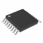 SN74HCS237QPWRQ1
The activity of extra discounts on wholesale prices is in full swing…
Please fill in your contact information and we will send you the latest wholesale price list.





