 ChipApex | Global Electronic Components Supplier
SEARCH
Search Product
Search Post
— IC芯片 | 连接器 | 传感器 | 被动器件 —
Search productSearch post
— IC芯片 | 连接器 | 传感器 | 被动器件 —
Consult the customer manager about the wholesale price.
consultation hotline:86-132-6715-2157
email:[email protected]
Contact the product manager for consultation. One-stop consultation is available.
Do you want a lower wholesale price? Please send us your inquiry and we will reply immediately.
The SN74HCS259QPWRQ1 is an automotive-grade, 8-bit addressable latch from Texas Instruments' HCS logic family. It operates within a supply voltage range of 2 V to 6 V and supports an ambient temperature range of -40°C to +125°C. The device features Schmitt-trigger inputs for noise tolerance and balanced CMOS push-pull outputs capable of ±7.8 mA drive current at 6 V. It includes a low-power design with typical supply current of 100 nA and input leakage of ±100 nA. Packaged in a 16-pin TSSOP, it provides eight active-high outputs controlled by three address select lines.
Verify the specific package variant against the datasheet orderable addendum, as the SN74HCS259-Q1 series includes multiple options such as TSSOP, SOIC, and wettable flank QFN. Confirm that the selected part matches the required thermal and electrical specifications for your target operating conditions. Ensure compliance with AEC-Q100 standards if deploying in automotive contexts.
Select this component when designing systems requiring general-purpose storage, working registers, or serial-holding registers. It is suitable for active-high decoders or demultiplexers where single-line data must be stored in eight addressable latches. Consider its wide voltage range and Schmitt-trigger inputs for applications involving noisy environments or slow input signals.
This device belongs to the SN74HCS259-Q1 family of automotive addressable latches. It shares functional similarities with other members of the HCS logic family but is specifically optimized for automotive reliability. The 'Q1' suffix indicates qualification for automotive applications, while the base model number defines the 8-bit latch functionality.
Consult the manufacturer's documentation for direct pin-compatible alternatives within the SN74HCS259-Q1 family. Verify that any substitute maintains the same voltage range, output drive capabilities, and Schmitt-trigger input characteristics to ensure system compatibility.
The device supports Addressable-latch mode (CLR=HIGH, G=LOW), Memory mode (CLR=HIGH, G=HIGH), 1-of-8 decoding/demultiplexing mode (CLR=LOW, G=LOW), and Clear mode (CLR=LOW, G=HIGH).
Unused inputs must not be left floating; they should be terminated to either VCC or ground using pull-up or pull-down resistors to prevent undefined operational states.
The device can drive a load with a total capacitance less than or equal to 50 pF while meeting all datasheet specifications.
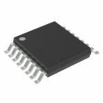 SN74HCS259QPWRQ1
The activity of extra discounts on wholesale prices is in full swing…
Please fill in your contact information and we will send you the latest wholesale price list.





