 ChipApex | Global Electronic Components Supplier
SEARCH
Search Product
Search Post
— IC芯片 | 连接器 | 传感器 | 被动器件 —
Search productSearch post
— IC芯片 | 连接器 | 传感器 | 被动器件 —
Consult the customer manager about the wholesale price.
consultation hotline:86-132-6715-2157
email:[email protected]
Contact the product manager for consultation. One-stop consultation is available.
Do you want a lower wholesale price? Please send us your inquiry and we will reply immediately.
The SN74HCS573-Q1 is an automotive-grade octal transparent D-type latch featuring Schmitt-trigger inputs and three-state outputs. It operates within a supply voltage range of 2 V to 6 V and supports an ambient temperature range from -40°C to +125°C. The device utilizes a flow-through pinout architecture for simplified bus routing. Electrical characteristics include a typical supply current of 100 nA, input leakage of ±100 nA, and output drive capability of ±7.8 mA at 6 V. Propagation delay ranges from 9.6 ns to 33 ns depending on voltage.
Verify the specific WRKS (VQFN) package variant matches the target footprint. Confirm AEC-Q100 qualification requirements align with the project's automotive grade specifications. Ensure the operating voltage range of 2 V to 6 V is compatible with the system power rails. Validate thermal management capabilities against the junction-to-ambient resistance values provided in the datasheet.
Select this component when designing automotive systems requiring robust noise immunity via Schmitt triggers. The wide voltage range accommodates various power architectures. The flow-through pinout is advantageous for dense board layouts. Consider the low static power consumption for battery-sensitive applications. Verify that the output drive strength meets the load requirements without exceeding absolute maximum ratings.
This part belongs to the SN74HCS series of high-speed CMOS logic devices designed for automotive environments. It functions as an octal latch, distinct from flip-flops or buffers. The 'Q1' suffix indicates automotive qualification. It shares the HCS logic family characteristics but is specifically optimized for the specified voltage and temperature ranges.
Consult the official Texas Instruments product selection guide for verified cross-references. Non-automotive equivalents like the standard SN74HCS573 lack the required qualification. Direct pin-compatible replacements must be confirmed through manufacturer documentation to ensure electrical and functional parity.
The Schmitt-trigger architecture introduces hysteresis, allowing the device to reject noise and accept slow-rising input signals without causing multiple transitions or excessive dynamic current consumption.
The flow-through pinout arranges inputs and outputs in a linear sequence (e.g., D1 to D8 followed by Q1 to Q8), which simplifies routing parallel data buses on printed circuit boards.
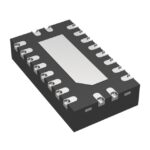 SN74HCS573QWRKSRQ1
The activity of extra discounts on wholesale prices is in full swing…
Please fill in your contact information and we will send you the latest wholesale price list.





