 ChipApex | Global Electronic Components Supplier

SEARCH
Search Product
Search Post
— IC芯片 | 连接器 | 传感器 | 被动器件 —
Search productSearch post
— IC芯片 | 连接器 | 传感器 | 被动器件 —
Consult the customer manager about the wholesale price.
consultation hotline:86-132-6715-2157
email:[email protected]
Contact the product manager for consultation. One-stop consultation is available.
Do you want a lower wholesale price? Please send us your inquiry and we will reply immediately.
SN74HCS595QBQBRQ1 is listed in the Shift Registers range at ChipApex. The manufacturer field lists Texas Instruments. Its product description is AUTOMOTIVE 8-BIT SHIFT REGISTER. Review the specifications below when checking this part for your BOM.
The SN74HCS595QBQBRQ1 is an automotive-grade, 8-bit serial-in, parallel-out shift register with a storage register and Schmitt-trigger inputs. It operates within a supply voltage range of 2 V to 6 V and features balanced CMOS 3-state outputs. The device supports cascading via a serial output (QH') and includes separate clocks for the shift and storage registers. It is qualified under AEC-Q100 standards for Grade 1 applications, functioning reliably across temperatures from -40°C to +125°C.
Verify that the specific WBQB package variant matches the wettable flank requirement for your assembly process. Confirm the AEC-Q100 Grade 1 qualification aligns with your vehicle's thermal and reliability specifications. Ensure input signal voltages remain within the absolute maximum ratings to prevent clamp diode damage during operation.
Select this component when a wide operating voltage range between 2 V and 6 V is required. The Schmitt-trigger architecture is essential for noisy automotive environments or slow signal transitions. Use this part if wettable flank packaging is mandated for enhanced solder joint inspection and reliability compared to standard QFN packages.
This device belongs to the SN74HCS595-Q1 family of automotive logic ICs. It shares functional compatibility with other HCS series shift registers but is distinguished by its specific WBQB package configuration. The family is designed to meet rigorous automotive quality standards while providing low power consumption and robust noise immunity.
SN74HCS595BQB-Q1
When the OE input is high, the storage register outputs enter a high-impedance state. However, internal register data and the serial output (QH') are not impacted by the OE operation.
The SRCLR input provides a direct overriding clear function for the shift register. When active low, it resets the shift register regardless of clock or serial input states.
Yes, the devices can be cascaded. The serial output (QH') of one device connects to the serial input (SER) of the next, allowing for extended bit shifting capabilities.
Explore related parts through Logic, Integrated Circuits (ICs), all product categories, ChipApex homepage.
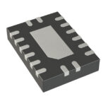 SN74HCS595QBQBRQ1

The activity of extra discounts on wholesale prices is in full swing…
Please fill in your contact information and we will send you the latest wholesale price list.






