 ChipApex | Global Electronic Components Supplier

SEARCH
Search Product
Search Post
— IC芯片 | 连接器 | 传感器 | 被动器件 —
Search productSearch post
— IC芯片 | 连接器 | 传感器 | 被动器件 —
Consult the customer manager about the wholesale price.
consultation hotline:86-132-6715-2157
email:[email protected]
Contact the product manager for consultation. One-stop consultation is available.
Do you want a lower wholesale price? Please send us your inquiry and we will reply immediately.
SN74HCT165QPWRQ1 is listed in the Shift Registers range at ChipApex. The manufacturer field lists Texas Instruments. Its product description is AUTOMOTIVE 8-BIT PARALLEL LOAD S. Review the specifications below when checking this part for your BOM.
The SN74HCT165QPWRQ1 is an automotive-grade, 8-bit parallel-load shift register manufactured by Texas Instruments. It operates within a supply voltage range of 4.5 V to 5.5 V and supports temperatures from -40°C to +125°C. The device features TTL-compatible inputs with VIH(min) at 2 V and VIL(max) at 0.8 V. It provides balanced CMOS push-pull outputs capable of driving up to 10 LSTTL loads. Key timing parameters include a maximum clock frequency of 31 MHz at 4.5 V and propagation delays ranging from 35 ns to 60 ns depending on the input source.
Verify that the specific ordering suffix matches the required package type and tape-and-reel specifications. Confirm AEC-Q100 qualification status is maintained for the intended automotive application environment. Ensure supply voltage constraints between 4.5 V and 5.5 V are strictly adhered to during system design validation.
Select this component when TTL-compatible logic levels are required for input signals. Choose this part for designs needing asynchronous parallel loading alongside serial shifting capabilities. Consider the thermal resistance metrics if operating near the upper temperature limits or under high capacitive loads exceeding typical values.
This device belongs to the SN74HCT165-Q1 family of automotive shift registers. It shares functional similarities with other parallel-load shift registers but is distinguished by its HCT logic family characteristics and specific automotive reliability certifications. It serves as a bridge between parallel peripheral data and serial microcontroller processing requirements.
SN74HCT165PW-Q1
When the SH/LD input is held low, the internal registers asynchronously load data from the parallel inputs A through H. When held high, the device shifts data on the rising edge of the clock pulse.
The CLK INH input acts as a clock inhibit signal. Holding it high prevents clock pulses from being detected, effectively pausing the shifting operation regardless of the state of the primary CLK input.
Explore related parts through Logic, Integrated Circuits (ICs), all product categories, ChipApex homepage.
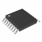 SN74HCT165QPWRQ1

The activity of extra discounts on wholesale prices is in full swing…
Please fill in your contact information and we will send you the latest wholesale price list.





