 ChipApex | Global Electronic Components Supplier

SEARCH
Search Product
Search Post
— IC芯片 | 连接器 | 传感器 | 被动器件 —
Search productSearch post
— IC芯片 | 连接器 | 传感器 | 被动器件 —
Consult the customer manager about the wholesale price.
consultation hotline:86-132-6715-2157
email:[email protected]
Contact the product manager for consultation. One-stop consultation is available.
Do you want a lower wholesale price? Please send us your inquiry and we will reply immediately.
SN74LS323DW is listed in the Shift Registers range at ChipApex. The manufacturer field lists Texas Instruments. Its product description is PARALLEL IN PARALLEL OUT. Review the specifications below when checking this part for your BOM.
The SN74LS323DW is an 8-bit universal shift/storage register manufactured by Texas Instruments in a 20-pin SOIC package. It operates within a DC supply voltage range of 4.75V to 5.25V and supports a maximum clock frequency of 40 MHz. The device features parallel-in/parallel-out capabilities with serial input options, providing eight data outputs capable of driving up to 8 mA. Propagation delay is specified at 27.0 ns, with an operating temperature range from 0°C to 70°C.
Verify the specific suffix 'DW' indicates the 20-pin SOIC package variant. Confirm RoHS compliance status as documentation may vary by production batch. Ensure the operating environment remains within the specified 0°C to 70°C temperature range for reliable performance. Cross-reference the manufacturer's latest datasheet for any updates to electrical characteristics or pin configurations before final integration.
Select this component when an 8-bit storage solution with both serial and parallel interfaces is required. The LS series offers standard speed suitable for general logic applications. Consider the 20-pin SOIC footprint for PCB layout compatibility. Verify that the 5V logic level requirements match the system design constraints.
This part belongs to the Texas Instruments SN74LSxx logic family, specifically designed for shift register functions. It serves as a universal shift/storage register, distinct from simple D-type flip-flops like the SN74LS273 or basic OR gates like the SN74LS32. The DW suffix denotes the plastic small-outline integrated circuit package type.
Compatible substitutes include other SN74LS323 variants such as SN74LS323N (PDIP) or SN74LS323DWR (tape and reel). Verify package dimensions and pinout compatibility before substitution.
Explore related parts through Logic, Integrated Circuits (ICs), all product categories, ChipApex homepage.
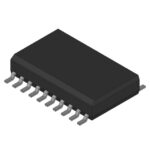 SN74LS323DW

The activity of extra discounts on wholesale prices is in full swing…
Please fill in your contact information and we will send you the latest wholesale price list.





