 ChipApex | Global Electronic Components Supplier
SEARCH
Search Product
Search Post
— IC芯片 | 连接器 | 传感器 | 被动器件 —
Search productSearch post
— IC芯片 | 连接器 | 传感器 | 被动器件 —
Consult the customer manager about the wholesale price.
consultation hotline:86-132-6715-2157
email:[email protected]
Contact the product manager for consultation. One-stop consultation is available.
Do you want a lower wholesale price? Please send us your inquiry and we will reply immediately.
The SN74LV157ANS is a quadruple 2-line to 1-line data selector/multiplexer from the SN74LV157A series. It operates within a supply voltage range of 2 V to 5.5 V and accepts input voltages up to 5.5 V. The device features a maximum propagation delay of 7.5 ns at 5 V and includes an active-low output strobe (G) input. It provides true data outputs and is designed for robust performance with latch-up characteristics exceeding 100 mA per JESD 78, Class II.
Verify the specific package suffix 'NS' corresponds to the SOP-16 configuration required for your design. Confirm that the operating temperature range of -40°C to +85°C aligns with your environmental specifications. Ensure input signals do not exceed the absolute maximum ratings to prevent damage. Check the latest orderable addendum for current production status and availability details.
Select this component when a quadruple multiplexer is needed with inputs compatible with 5.5 V logic levels while operating on lower supply voltages. The LV157A offers faster switching speeds compared to standard LV devices. Consider the SOP-16 package constraints regarding board space and thermal dissipation requirements for your specific application layout.
This part belongs to the SN74LV157A family of quadruple 2-line to 1-line data selectors. These devices are CMOS-based logic ICs designed for high-speed data routing applications. The family supports various packages including SSOP, TVSOP, SOIC, SOP, and TSSOP, providing flexibility for different PCB mounting needs and density requirements.
SN74LV157ADBR
The G pin is an active-low output strobe. When G is high, all outputs are forced low regardless of other inputs. When G is low, the selected data inputs are routed to the outputs.
The latch-up performance exceeds 100 mA per JESD 78, Class II, ensuring robust protection against latch-up events under specified test conditions.
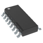 SN74LV157ANS
The activity of extra discounts on wholesale prices is in full swing…
Please fill in your contact information and we will send you the latest wholesale price list.





