 ChipApex | Global Electronic Components Supplier

SEARCH
Search Product
Search Post
— IC芯片 | 连接器 | 传感器 | 被动器件 —
Search productSearch post
— IC芯片 | 连接器 | 传感器 | 被动器件 —
Consult the customer manager about the wholesale price.
consultation hotline:86-132-6715-2157
email:[email protected]
Contact the product manager for consultation. One-stop consultation is available.
Do you want a lower wholesale price? Please send us your inquiry and we will reply immediately.
SN74LV165APWRE4 is listed in the Shift Registers range at ChipApex. The manufacturer field lists Texas Instruments. Its product description is IC REGISTR PAR-LOAD 8BIT 16TSSOP. Review the specifications below when checking this part for your BOM.
The SN74LV165APWRE4 is a parallel-load, 8-bit shift register from the Texas Instruments SN74LV165A family. It operates on a supply voltage (VCC) ranging from 2 V to 5.5 V and supports mixed-mode voltage operation across all ports. The device features eight direct data inputs enabled by a low level at the shift/load (SH/LD) pin. Data shifts toward the serial output QH when clocked with SH/LD held high and CLK INH held low. It includes a clock-inhibit function and complemented serial output.
Verify the specific ordering suffix 'PWRE4' against the manufacturer's official orderable addendum to confirm package type and tape-and-reel configuration. Ensure the component meets RoHS3 compliance standards as indicated in the datasheet specifications. Confirm availability status directly through authorized distribution channels prior to procurement planning.
Select this component for designs requiring parallel-to-serial conversion within a 2 V to 5.5 V operating range. Consider the TSSOP-16 package dimensions if space constraints apply. Evaluate the maximum propagation delay requirements against system timing budgets. Verify that input transition rates meet the recommended conditions to prevent oscillation or excessive power consumption during operation.
This part belongs to the SN74LV165A series of parallel-load 8-bit shift registers manufactured by Texas Instruments. The LV designation indicates Low-Voltage CMOS technology compatible with various logic families. The RE4 suffix typically denotes environmental compliance and packaging format variations within the standard product line.
Consult the SN74LV165A datasheet orderable addendum for verified substitute part numbers sharing identical electrical characteristics and pinouts. Cross-reference package options such as SOIC, SSOP, or TVSOP if physical footprint modifications are permissible in the design.
The device utilizes Ioff circuitry to disable all outputs when the supply pin is held at 0 V, preventing damaging current backflow regardless of applied input voltages.
The shift/load (SH/LD) input enables parallel access to each stage when held at a low level; holding it high inhibits parallel loading and allows shifting operations.
Explore related parts through Logic, Integrated Circuits (ICs), all product categories, ChipApex homepage.
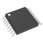 SN74LV165APWRE4

The activity of extra discounts on wholesale prices is in full swing…
Please fill in your contact information and we will send you the latest wholesale price list.





